

VLSI Technology is all about creating complex chips and SoCs by packing billions of transistors into a single chip. The chips are extensively used in various sectors like data centres, telecommunications, automotive, defense, consumer electronics, industrial automation etc. Designing these tiny chips containing very complex circuitry built with billions of transistors is not a simple job, nor a one-step process. These chips, particularly ASICs can be designed by using either Full-Custom or Semi-Custom design methodologies.
In the case of Full Custom Design Methodology, it is required to design and verify all the logic components right from the transistor level, by customizing the length & width of the transistors and by customizing how floor planning & routing are done. This customization helps us to obtain the required characteristics in terms of power consumption, area of the chip, and propagation delays of the logic components. Since the pre-designed standard cells are not used in this methodology, design time, complexity, and cost for the design are more. So, this design methodology is best suited for mass production. In this methodology, SPICE Modelling is used for characterization.
In the case of Semi-Custom Design Methodology, pre-designed, pre-tested, and pre-characterized standard cells are used to design the circuitry by integrating additional components which are not available in the standard cell library. This design methodology will save a lot of design time, but the design will not be an optimized design with the required characteristics such as propagation delay, area, and power consumption. This design methodology can be used if the time to market is critical and for lesser quantities.
In this article, let me explain the full custom design flow which involves the physical design of transistors of the circuit and the interconnectivity between these transistors. Physical Design is a process of converting the RTL netlist into a layout that is manufacture-able (GDS). And this process of converting a netlist into a manufacture-able layout involves multiple steps as shown below.
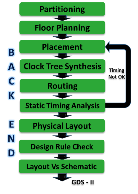

Partitioning: It involves the decomposition of a complex circuit into smaller subsystems (sub-blocks) so that each subsystem will be of a manageable size and the no. of interconnections between these sub-blocks will be minimum.
Floor planning: In this step, the rough position of each block on the silicon chip and the shape of each block will be decided. And also, the pin locations of each block will be decided so that the interconnections between these blocks can be routed easily in the future as shown in the below picture.
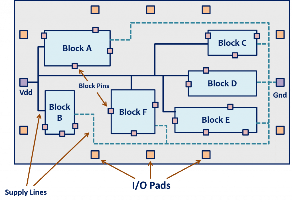

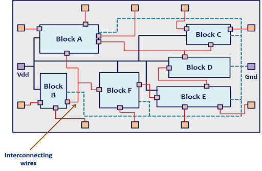
Placement: In this step, the exact position of various sub-blocks will be decided with the objective of maintaining adequate space between various blocks, so that, Vdd and Ground supply lines and the interconnection wires can be routed in such a way that, there will be no clutter as shown in the above figure.
Clock Tree Synthesis (CTS): After the completion of floor planning and placement, millions of flip-flops in the complex circuit will be scattered at multiple places on the silicon chip, so that the transmission delays of the clock signal for all the flip-flops will not be the same. The clock will not arrive/reach all the flip-flops at the same time as shown in the figure below. The difference in the arrival times of the clock signal to these flip-flops is referred to as clock skew.
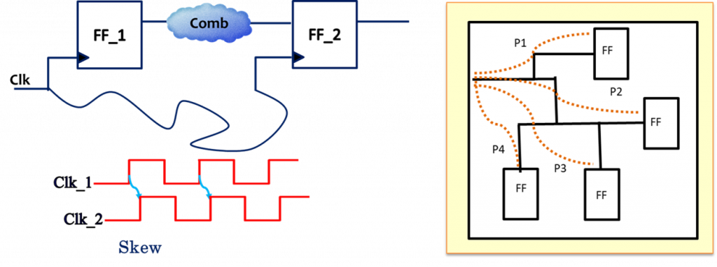

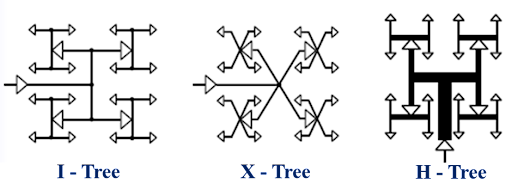
And it is mandatory to make sure that, the clock signal reaches multiple flip-flops with no or minimum skew difference. CTS will ensure that the clock reaches various flip-flops almost at the same time. In the clock tree synthesis process, any one of the standard Tree topology structures (shown in the below picture) will be implemented in the design with an intention of making the length of all the wires in the clock distribution network equal.

Routing: In this step, interconnecting wires between various blocks will be routed in such a way that, the length of the interconnecting wires will be minimum for meeting the timing requirements and for ensuring that, the chip area will not be increased as shown in the below picture. Proper routing will also ensure that there are no congestion hotspots in the chip so that, the probability of having faults during the fabrication will be less.

Static Timing Analysis: Static Timing Analysis will be done on the final routed netlist which will represent/mimic the final layout of the chip that is going to be fabricated for validating the timing performance of the chip and to ensure that, the chip will meet the timing requirements such as maximum frequency of operation and the design works fine at the desired frequency without any setup and hold time violations.
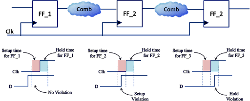

If the timing requirements are not met or if there are any setup and hold time violations identified, then, optimizing the placement and routing will be done, so that, timing may be improved, and violations will be eliminated.
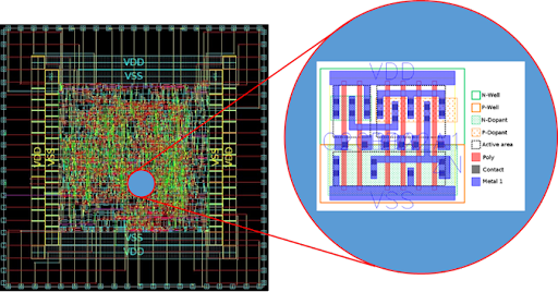
Post the timing requirements are satisfied, the physical layout as shown below will be extracted, and these layouts will be used during the fabrication to prepare the required mask layers which will be used in the photolithography processes.

Design Rule Check: The physical layout must obey the design rules imposed by the foundry to ensure that, the layout is manufacturable with a minimum no. of fabrication faults. They act as an interface or communication link between the circuit designer and the process engineer during the manufacturing phase. So, to ensure that the layout obeys all the design rules, a DRC will be done.
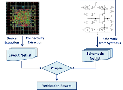
Layout Vs Schematic: Finally, to ensure that the design’s functionality is not altered during the physical design implementation Layout, the Layout Vs Schematic (LVS) equivalence checking as shown in the below picture will be done. This equivalence as shown below will be able to identify if there are missing device terminals or extra device terminals or unmatched devices and nets in the layout/schematic.

Once this implementation flow which includes floor planning, placement, CTS, Routing, and Signoff flow with DRC and LVS is completed, the final GDS-II file will be sent to the foundry where the actual silicon chips are created through a fabrication process using Silicon wafer.
As explained so far, the physical design flow contains several stages which require the effort of many skilled VLSI engineers at each stage. So, the demand for skilled VLSI Physical Design Engineers will continue to grow as the demand for ICs is raising at a fast pace.
If you’re aspiring to become a Physical Design & Verification Engineer, VLSI Physical Design Course with 100% placement assistance.


3 Comments
Comments are closed.