
We need more and more complex chips and SoCs for all new applications that use the latest technologies like AI. For example, Apple’s 5nm SoC A14 features 6-core CPU, 4 core-GPU and 16-core neural engine capable of 11 trillion operations per second, which incorporates 11.8 billion transistors, and AWS 7nm 64-bit Graviton2 custom processor contains 30 billion transistors. Designing such complex chips demands a standard and proven verification flow that involves extensive verification at every level, block to IP to Sub-system to SoC, using various verification methodologies and technologies.
In this article, let me walk you through various verification methodologies we use for verifying IPs, Sub-systems, and SoCs and explain why we need new methodologies/standards like PSS.
Understanding how we build electronic systems using SoCs is essential for the verification engineers who deal with SoC verification flow, whether doing a white-box verification at the IP level, gray-box verification at the sub-system level, or black-box verification at the SoC level.
How do we build electronic systems using SoC?
Any chip, a simple embedded microcontroller, or a complex system-on-a-chip [SoC] will have one or more processors. Figure1 shows a complex electronic system composed of both hardware and software needed for electronic devices like smartphones.


Electronic System
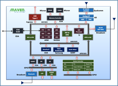

Figure 1 : Electronic System and System-On-Chip
The hardware is made up of a complex SoC that incorporates almost all the components needed for the device. In the case of the smartphone, we integrate all the hardware components called IPs [Intellectual Properties] like CPUs, GPUs, DSP, Application Processors, Interface IPs like USB, UART, SPI, I2C, GPIO, and subsystems like System Controllers, Memories with controllers, Bluetooth, and WiFi, etc. and create the SoC. Using SoC helps us to reduce the size and power consumption of the device while improving its performance.
The software is composed of application software and system software. The application software provides the user interface, and the system software provides the interface to the application software to deal with the hardware. In the smartphone case, the application software could be mobile apps like YouTube, Netflix, GoogleMap, etc, and the system software could be the operating system [OS] like ios or android. The system software provides everything like firmware and protocol stack along with the OS needed for the application software to interface with the hardware. The OS manages multiple application threads in parallel, memory allocation, and I/O operations as a central component of the system software.
Let me explain how the entire system, like a smartphone works. For example, when you invoke an application like a calculator on a smartphone, the operating system loads the executable binary from the storage memory into RAM. Then it immediately loads its starting address into the program counter [PC] of its processor. The processor [ARM/x86/RISC-V] executes the binary loaded in the RAM/Cache pointed by the PC [address of RAM]. This precompiled binary is nothing but the machine language of the processor, and therefore the processor executes the application in terms of its instructions [ADD/SUB/MULT/LOAD] and calculates the results.
Understanding the SoC design process using processors can help the verification engineers deal with any complex sub-system/chip verification at the system level. As part of the SoC verification process, verification engineers may need to deal with various things like virtual prototyping for system modeling, IP, subsystem and SoC functional verification, hardware-software co-verification, emulation, ASIC prototyping, post-silicon validation, etc. in their long-term career. So it demands a cohesive and complete knowledge and understanding of both hardware and software to work independently as verification experts and sometimes to work closely with software teams as well to deal with the software, RTOS/firmware/stacks for the chip/system level verification.
Now let us explore various verification methodologies.
IP Verification
IPs are the fundamental building blocks for any SoC. So IP verification demands exhaustive white-box verification that demands methodologies like formal verification and random simulation, especially for the processor IPs as everything is initiated and driven by them as a central component in any SoCs. Figure 2 shows how we verify a processor IP using an exhaustive random simulation by a SystemVerilog-based UVM TB. All the processor instructions can be simulated with various random values, generating functional, assertion, and code coverage. We use coverage to measure the progress and quality of the verification and then for the final verification sign-off. IP level verification demands good expertise in HVL programming, Formal and Dynamic ABV, Simulation debugging, and using VIPs and EDA tools.
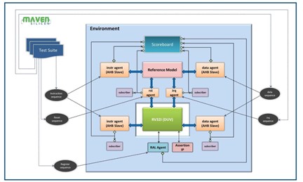

Figure 2: RISC-V UVM Verification Environment
ABV- Assertion Based Verification, VIP – Verification IP
UVM-Universal Verification Methodology UVC-UVM Verification component
BFM-Bus Functional Model VIP-Verification IP RAL-Register Abstraction Layer
Sub-System Verification
Sub-systems are composed of mostly pre-verified IPs and some newly built IPs like bridges and system controllers that are specific to the chip. Figure 3 shows how we build an SoC from a sub-system that integrates all the necessary interface IPs, bridges, and system controllers using an on-chip bus like AMBA. In this case, we prefer simulation-based Gray-box verification, especially random simulation using verification IPs. All the VIPs like AXI, AHB, APB, GPIO, UART, SPI, and I2C UVCs [UVM Verification Component] will be configured and connected with the respective interfaces. As shown in the figure-3, we create other TB components like reference models, scoreboards, and UVM RAL for making the verification environment self-checking. We execute various VIP UVM sequences at the top level, verify the data flow, and measure the performance of the bus.
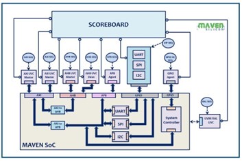

Figure 3: Sub-System UVM Verification Environment
SoC Verification
SoCs are composed of primarily pre-verified third-party IPs and some in-house IPs. Usually, we prefer a black-box verification using hardware emulation or simulation technologies for the SoC level verification. For example, you may come across a complex SoC verification environment, as shown in figure 4. The SoC testbench [TB] will have all kinds of testbench components like standard UVM Verification IPs[USB/Bluetooth/WiFi and standard interfaces], legacy HDL TB components [JTAG Agent] with UVM wrappers, custom UVM agents[Firmware agents], and some monitors, in addition to the scoreboard and SystemC/C/C++ functional models. In this case, you will have to deal with both firmware and UVM sequences at the chip level. As a verification engineer, you need to know how to implement this kind of hybrid verification environment using the standard VIPs, legacy HDL BFMs and firmware code, and more importantly, how to automate the simulation/emulation using EDA tools.
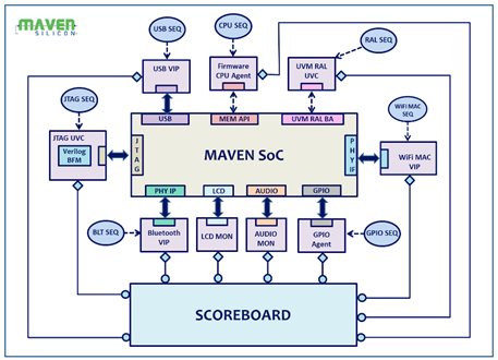

Figure 4: SoC Verification Environment
UVM-Universal Verification Methodology UVC-UVM Verification component
BFM-Bus Functional Model VIP-Verification IP RAL-Register Abstraction Layer
Let me explain how it works. For example, if the SoC uses an ARM processor, usually we replace the ARM RTL [Encrypted Netlist/RTL] with its functional model called DSM [Design Simulation Model] that can use the firmware[Written in C] as a stimulus to initiate any operation and drive all other peripherals[RTL IPs]. So the SoC verification folks write UVM sequences to generate various directed scenarios through firmware testcases and verify the SoC functionality. During the simulation, the firmware C source code is compiled as an object code[ARM Machine Language binary] which will be loaded into on-chip RAM. The ARM processor model [DSM] reads the object code from memory and initiates the operation by configuring & driving all the RTL peripheral blocks [Verilog/VHDL]. It works for both simulation and emulation. If the SoC is very complex, hardware emulation is preferred to accelerate the verification process and achieve faster verification sign-off.
Why PSS?
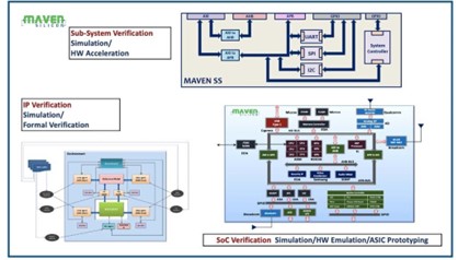

Figure 5: IP, Sub-System, and SoC Verification Methodologies
PSS Definition: The Portable Test and Stimulus Standard defines a specification for creating a single representation of stimulus and test scenarios, usable by a variety of users across different levels of integration under different configurations, enabling the generation of different implementations of a scenario that run on a variety of execution platforms, including, but not necessarily limited to, simulation, emulation, FPGA prototyping, and post-Silicon. With this standard, users can specify a set of behaviors once, from which multiple implementations may be derived.
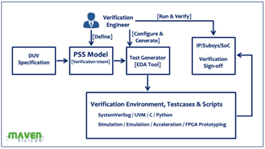

Figure 6 : PSS flow
As shown in figure6, using PSS, we can define the test scenarios and execute them at any level IP/Sub-System/SoC using any Verification Technology. For example, we can define an IP’s test scenarios in PSS. At the IP level verification, we can generate assertions using EDA from its PSS specification for the formal verification, and if needed, we can generate UVM testcases from the same PSS specification for the simulation or emulation at the SoC level. We don’t need to manually rewrite the IP/Sub-system level testcases to migrate and reuse them at the SoC level. PSS specification remains the same for all kinds of technologies. Based on our choice, like formal/simulation/emulation, the EDA tool can generate the testcases from PSS speciation in any languages or methodologies like C/C++/Verilog/SystemVerilog/UVM.
The methodologies like formal verification and PSS are evolving, simultaneously the EDA vendors are also automating the test generation and verification sign-off using technologies like ML. So in the near future, the industry needs brilliant and skilled verification engineers who can collaborate with the chip architects to drive the verification process for the first-time silicon success through the ‘Correct by Construction’ approach, beyond the traditional verification folks who deal with black-box verification that involves predominantly writing testcases and managing the regression testing. Are you interested in chip verification and ready for this big job?
To learn more about SoC Design & Verification methodologies, explore our course on Advanced VLSI Design & Verification.