

I am glad to address this question and explain to those who might always be wondering and asking everyone in the industry ‘Where are we heading?’
We are heading towards the smart world that offers smart homes, smart cities, and industrial and business automation through IoT and artificial intelligence. It’s possible primarily because of new and powerful chips that we make with the help of advanced fabrication process, along with new and powerful software applications that we create with the help of advance software programming technologies and platforms.
Let us recollect how our journey has been with the evolution of chip design. But I don’t want to simply go all the way back to our old life with the radio made up of vacuum tubes. We can start with our life integrated with Music System, Telephone & Television two decades back. If you recollect your memories well, later on, personal computers became popular and replaced many devices like music systems, typing machines, etc. and introduced automation in every business and industry. Then we transformed the PCs into laptops mainly through the advancement of chip design technology like SoC [System-On-Chip] design. With this experience, we were able to create smartphones and tablets. This empowered every common man to create and share data with the world, mainly with the help of the internet through social media platforms like Facebook, YouTube, WhatsApp, Twitter, etc. So, I would say, the advancement of software programming technologies on par with the chip design too helped us to reach this current state.
Naturally, this empowerment [Powerful Hardware + Powerful Software] leads us to realize the smart world through the evolution of technologies like the Internet of Things and Artificial Intelligence. So, in this article, I would like to explain how this new era of automation is going to transform the semiconductor industry.
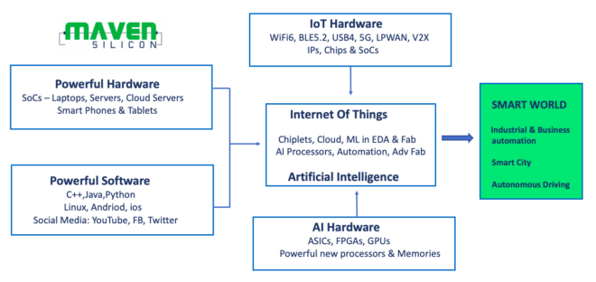

Internet of Things [IoT/IoE] demands new standards of connectivity protocols like WiFi6, BLE5.2, USB4, 5G, LPWAN, V2X, etc. to realize the Industrial Automation, Smart City, Autonomous Driving, etc. In order to support the new standards and protocols, we chip designers need to design and create new IPs, Chips, and SoCs at higher technology nodes. Some automotive and industrial chips may demand a specialized fabrication process, as they may be used in unusual environments.
Artificial Intelligence demands powerful processors and memories to realize applications like Autonomous Driving, Natural Language Processing [NLP], Machine Learning [ML], etc. The growth and amount of real-time data collected from the IoT enabled devices and the advancement of machine learning algorithms on devices and cloud will lead to the growth of AI-based applications. NLP, automation, and trust are the three main themes that will shape the advancement of AI.
At present, AI experts are open to trying everything, new & existing processors, FPGAs, GPUs, etc. For some mathematical intensive applications, they find FPGAs are better than ASICs. As long as their software works fine at high throughput and optimal power and they are fine to try and use any piece of silicon, ASIC/FPGA, to create the AI application at the right cost. So, I would say the evolution of new processors and memories only can help AI experts to standardize the implementation process and create many new AI applications at an optimal price.
It’s obvious that the evolution of AI and IoT demands new and powerful Chips and SoCs. So, in the semiconductor industry, we are also exploring the options of creating such powerful SoCs through new design approaches like Chiplets in addition to the monolithic design process. As the monolithic SoC scale-up is expensive, we create the SoCs by directly connecting the chips which have already been fabricated at different technology nodes. There are several approaches to chiplets. The basic idea is that you have a menu of modular chips, or chiplets, in a library. Then, you assemble chiplets in a package and connect them using a die-to-die interconnect scheme. In theory, the chiplet approach is a fast and less expensive way to assemble various types of third-party chips, such as I/Os, memory, and processor cores, in a package.
Also, we opt for the cloud to design such complex SoCs that demand more computation during simulation or implementation. During peak load on the server firm especially while doing multiple tape-outs, any regression simulation or physical verification like DRC, LVS, etc may demand infinite additional hardware resources to sign-off the verification and meet TTM. So naturally, we move towards using the cloud for the chip design similar to software programming, as the EDA industry too offers cloud-based EDA solutions, addressing the IP security challenges.
We also use ML algorithms to improve the EDA process and do the chip design efficiently. ML algorithms are used to improve the EDA tool algorithms to automate and improve the performance in some areas like test generation, synthesis, physical design, etc. So, the evolution of AI transforms the chip design process too, while demanding and pushing us to create new and powerful chips.