
What is CDC?
Today’s device needs multiple clocks with increasing system integration, peripherals & external interfaces, and power management. In a design with multiple clocks, clock domain crossing occurs whenever data is transferred from a flip-flop driven by one clock to a flip-flop driven by another clock. When the signal is sampled in another clock domain and if there is any setup and hold time violation, the receiving register may become metastable and the output settles to some random value after an unknown amount of time.

Effects of Metastability
Since the CDC signal can fluctuate for some period of time, the input logic in the receiving clock domain might recognize the logic level of the fluctuating signal to be different values and hence propagate erroneous signals into the receiving clock domain. If the unstable data is fed to several other places in the design, it may also lead to a high current flow and even chip burnout in the worst case.
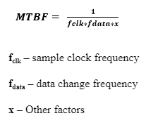
In a multi-clock design, metastability cannot be avoided but the detrimental effects of metastability can be neutralized by adding synchronizers. Today’s SOC can have >104 CDC signals on a single chip. Mean time before failure (MTBF) tells us how frequently the storage element can become metastable. Larger MTBF indicates longer time periods between failures, while smaller MTBF indicates that metastability can happen frequently.

Different Types of Synchronizers
The synchronizer avoids sampling metastable signals at the destination. Different types of synchronization structures are available, and each structure has strict rules for implementation that should be verified. In this paper, the most commonly used synchronizers are discussed.
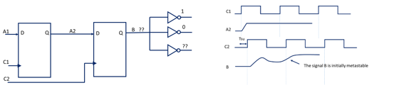
Multi-flop Synchronizer
The most used synchronizer is the multi-flop synchronizer shown in the below diagram
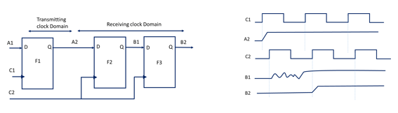

By adding synchronizer Flip flop in the destination domain, it allows sufficient time for the oscillations to settle down and ensure that a stable output is obtained in the destination domain by preventing the sampling of metastable signal. These multi-flop synchronizers can be used in the path of single-bit control signals.
Protocol to be taken care of for Multi-Flop Synchronizer
The glitch-free output should be driven from the transmitting clock domain to receiving clock domain, i.e., always the registered output from the transmitting clock domain should be driven to receiving clock domain and no combinational logic should be added between sending & receiving flipflops to avoid glitches. Do not place any combinational logic between synchronizer flip-flops to reduce the probability of metastability effect by reducing propagation delay between synchronizer flip-flops
Toggle Synchronizer
If the control signal changes too fast then the multi-flop synchronizer cannot avoid the sampling of a metastable signal at the receiving clock domain. In this case, we can use Toggle synchronizer as shown in the below diagram. The basic function of a pulse synchronizer is to take a single clock wide pulse from one clock domain and create a single clock wide pulse in the new domain.
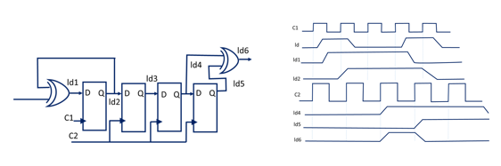

Protocol to be taken care of for Toggle Synchronizer
One restriction of a pulse synchronizer is that input pulses must have a minimum spacing between pulses equal to two synchronizer clock periods. If the input pulses are closer, the output pulses in the new clock domain are adjacent to each other, resulting in an output pulse that is wider than one clock cycle.
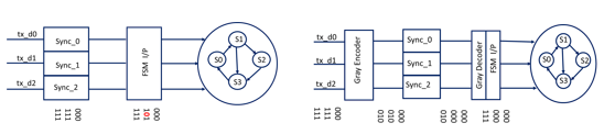
Gray Encoding
Consider a case as shown in the example where the input to the FSM is driven through synchronizers. The change in multiple bits at the same time may cause misalignment in the bus due to unpredictable delays in CDC paths, and the bus may go to illegal values and the state machine may hang. To prevent this issue we can use gray coding logic to the bus & this will prevent illegal values to occur. Now when the multiple bit changes at same time, the illegal value will not happen, but it will add unexpected delay.

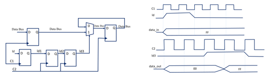
Mux Synchronizer
Suppose we have data of 16 bits to transfer from one clock domain to another clock domain, we cannot add synchronizers in the data path for all the 16 bits as it increases the size of the chip. In this case we can add synchronizers in the control path.
Transmitter domain is responsible to keep data stable on the bus when captured by the receiving domain (when sel of mux signal is asserted)

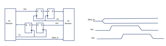
Handshaking Data between Clock Domains
The transmitter working on the C1 clock domain places data onto a data bus and then synchronizes a “req” signal (request) to the receiving clock (c2) domain. The “req” signal is recognized in the destination clock domain, the receiver clocks the data into a register (the data should have been stable for at least two/three sampling clock edges in the destination clock domain) and then passes an “ack” signal (acknowledgement) through a synchronizer to the sender. When the sender recognizes the synchronized “ack” signal, the sender can de-assert the “req” signal, then the receiver also de-asserts the “ack” signal to inform the sender that it is ready to accept another data. The sender can again start the handshaking process
With this technique, it is required that the receiving clock domain have logic in place to capture the data when the pulse is detected, because the pulse will only be valid for one receiving clock cycle per multi-cycle data word.

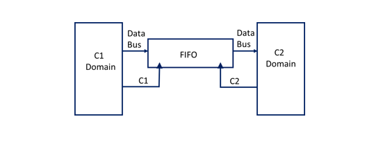
FIFOS
Asynchronous FIFO can be used to transmit data between two clock domains. Write operation to FIFO will happen in the clock C1 domain. Read operation from FIFO will happen in clock C2 domain. FIFO depth should be taken care based on frequency of the clocks C1 and C2

Even after adding all the synchronization techniques, still, there will be some errors. Traditional methods like simulation and static timing analysis alone are not sufficient to verify that the data is transferred consistently and reliably across clock domains. They are found late in the development cycle, usually only in silicon. Silicon Failures are intermittent, difficult to reproduce the same error.
Types of CDC errors
Synchronization errors – The errors caused by improper or missing synchronizers
CDC Transfer Protocol errors – The errors caused by violation of protocols of the synchronization structure
CDC reconvergence errors – The errors caused by non – deterministic delays of CDC signals to settle to a stable value
CDC Analysis Flow
Structural Analysis: Structural analysis must identify Different clock domains, CDC signals, and Synchronizers. It reports incorrect or missing synchronizers.
CDC Protocol Verification: During structural analysis only limited amount of protocol checking will happen. For unproven protocols assertions are created in the existing verification environment. The assertions can be verified with simulation or formal verification
Reconvergence Verification: It involves modelling dynamic delays caused by metastability. Behavioural model will model silicon accurate metastability with behaviour in simulation. By modelling this delay designers can identify reconvergence logic that is incorrect in that the logic is not tolerant to the metastability delays
Why CDC for your VLSI Career?
The semiconductor industry needs dedicated VLSI engineers who specialize in CDC verification, in addition to the regular verification engineers, as most of the current chips and SoCs are complex enough to have CDC by default with multiple clock domains. The CDC verification demands different verification methodologies like rule checking, simulation, STA, formal verification, etc. So learning CDC verification techniques along with RTL design and verification methodologies will help the electronics engineers to enter the Semiconductor Industry quickly, projecting their CDC verification skills as an added advantage. Are you the next CDC Expert we have been searching for?
If you’re aspiring to become a Verification Engineer, explore our Advanced ASIC Verification Course to learn different verification methodologies like rule checking, simulation, STA, formal verification, etc. along with Clock Domain Crossing.