
VLSI Technology is all about packing billions of transistors onto a single chip for creating complex SoCs. Designing these tiny chips containing very complex circuitry built with billions of transistors is not a simple job nor a one-step process. I strongly recommend the readers who are new to VLSI Physical Design should go through my previous article Physical Design Flow before reading this article to understand the physical synthesis process.
What is Practical Physical Synthesis?
In this article, let me explain the Synthesis processes from a practical perspective. The list of different inputs required and outputs generated by the physical synthesis process is shown in the figure below.
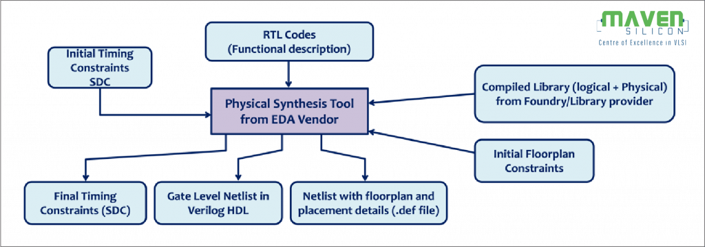

Since the modern-day ICs contain very complex circuitry, designing such complex circuits which contain millions of gates and flip-flops manually, is impossible. So, the design process is automated using Synthesis Process. Synthesis is a process of converting the RTL (Behavioural Register Transfer Level code) into an optimized Gate Level Netlist and finally, the synthesis process will map the gates and other digital logic blocks such as flipflops in the netlist with the equivalent blocks existing in the standard cell library.
![]()

The netlist generated by the synthesis tool will be used as input for the implementation(P&R) tool for performing floor planning, placement, and routing. But, if the routed netlist doesn’t meet the timing and power requirements, then we may need to go back to synthesis and optimize the netlist again. This may lead to many no. of iterations between the synthesis tool and the P&R[Placement & Routing] tool which will delay the time to market. To minimize the no. of iterations between synthesis and P&R tools, it is a good idea to do the initial level of floor-planning and placement during synthesis itself. The modern synthesis EDA tools are capable of generating Gate Level Netlist and initial floor-planning & placement data which will be acting as input for the P&R tool for more accurate placement and routing.
We will look into an example to understand more about Translation, Optimization, and Mapping in the later part of this article. During the Synthesis process, the standard cell library is one of the mandatory inputs to be supplied so that, it will be used in the Mapping process.
As mentioned earlier, VLSI Technology is all about packing billions of transistors onto a single chip for creating complex SoCs which will be used in highspeed computing, cloud systems, telecommunications, Automotives, defence, image and video processing, consumer electronics, Artificial Intelligence, etc. All the chips that will be used in a wide range of applications do not demand the same set of characteristics such as speed, area of the Silicon chip, Power consumption, and operating conditions.
For example, the chips that will be used in high-speed computing devices such as cloud servers, and Automotives, will demand the chips to work at high speed/frequency, consuming less power. But, the chips that are going to be used in portable and battery-operated gadgets such as smartwatches and other wearables, should not occupy more silicon area and should not consume more power, though the speed varies and it depends on the application. Similarly, the chips that will be used in applications, such as defence (radar equipment, sub-marines) and avionics should be designed in such a way that they can be operated in extreme climatic conditions such as high and low temperatures. So, the same type of logic cells such as gates, multiplexers, and flip-flops with the same characteristics (such as speed, area, power consumption, operating voltage, and operating temperature) are not suitable for all kinds of applications.
So, to meet the requirements of various applications as mentioned earlier, the standard cell libraries (which are available in PDKs[Process Design Kit] provided by foundries or library providers) come with predefined, pre-characterized logic gates and logic blocks in different variants. For example, if a standard cell library contains a two-input NAND gate, the same 2 input NAND gate will be available in multiple variants as listed below.
- Multiple Driving Strength: Gates with lesser driving strength, will consume less power, and occupy a lesser area, but operate with a higher propagation delay when compared with the gates with higher driving strength. The standard cell library contains the same NAND gate with multiple driving strengths.
- Multi-VT Cells: Similarly, the same NAND gate will be available with different threshold voltages such as LVT(Low Threshold Voltage), SVT (Standard Threshold Voltage), and HVT(High Threshold Voltage). LVT cells will have a lesser delay but operate with a higher leakage power consumption when compared with HVT cells.
- Multi-Vdd Cells: Gates with higher Vdd can operate with high speed, but, they consume more power at the same time.
- Multiple Operating Temperatures: Similarly, the same NAND gate will be available in different variants which are capable of working at different temperatures.
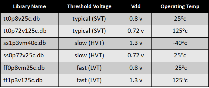
By looking at the library name, we can understand the characteristics of the logic cells available in a specific library. Please find below the table for the list of a few libraries that exist in a sample PDK from the foundry/library provider.

Depending upon the requirements such as PPA[Power, Performance, and Area] of the IC, and operating temperature, we will guide the synthesis tool to use the gates/logic blocks from a specific target library, or sometimes, we will use logic cells from different libraries for different blocks in an IC. For example, we will use logic cells from a slower library in the non-critical paths of the circuit so that, power consumption can be reduced and we will try to use logic cells from a faster library in the critical paths of the circuit, so that, speed can be improved.
The synthesis tool will take decisions on “which of the logic cells must be used while generating a netlist based on the PPA requirement”. Along with the standard cell libraries and the RTL code, initial floor planning constraints and timing & Power constraints (SDC) should also be supplied as additional inputs for the synthesis tools.
The initial Floor planning constraints file contains some constraints which will be used by the synthesis tool to take some of the decisions as described below.
- The maximum area of the chip and the shape of the chip: With this constraint definition, the synthesis tool understands the maximum area that can be occupied by the chip. If the maximum area that can be occupied should be very minimum, the synthesis tool will use smaller logic cells with less driving strength.
- Percentage of utilization: It represents the maximum area that can be utilized by the standard cell logic cells so that the remaining area of the chip can be used for routing the interconnecting wires in the future during the Routing stage. If the selected logic cells are utilizing more area when compared with this specified limit, then the synthesis tool will try to use much smaller logic cells from the library.
- The exact location of some of the blocks or macros on the chip: With this constraint definition, the synthesis tool understands and determines the exact location of some of the blocks on the chip. Since the exact location of some of the blocks is determined during Synthesis itself, the synthesis tool can estimate the power and timing characteristics more accurately.
Similarly, the SDC file which will be defined to provide design intent such as maximum speed required and maximum power consumption of the chip contains the definitions of some constraints as described below.
- Clock Time Period based on the maximum frequency required: with this definition, the synthesis tool can do an initial level of timing analysis and cross-checks, whether the netlist generated by the synthesis tool is working at the desired frequency without any setup and hold violations or not. This constraint will also guide the synthesis tool to decide which logic cell must be used (high-speed logic cell or low-speed logic cell) and to decide the location of various blocks. For example, if two or more logic blocks are placed very close to each other, then, the synthesis tool tries to place them far from each other in such a way that, the timing requirements and area requirements are still satisfied, so that, there is more space left between those blocks for proper routing without any congestion.
- The clock uncertainties such as jitter, and operating conditions such as temperature: These constraints will help the tool to do the timing and power analysis more accurately.
- The maximum allowable dynamic and leakage power: These constraints will help the tool to decide which logic cells (low-power cells or high-speed calls) to be chosen while generating the netlist.
- Timing Exceptions such as multi-cycle and false paths: These constraints will guide the Timing Analysis Engine of the synthesis tool about the list of paths to be exempted from doing timing analysis and reporting the violations.
Now, let’s look into the following example RTL code to understand how exactly the synthesis process will go on. After initiating the synthesis process, the RTL code will be translated into a gate-level circuit as shown below (Step 1).
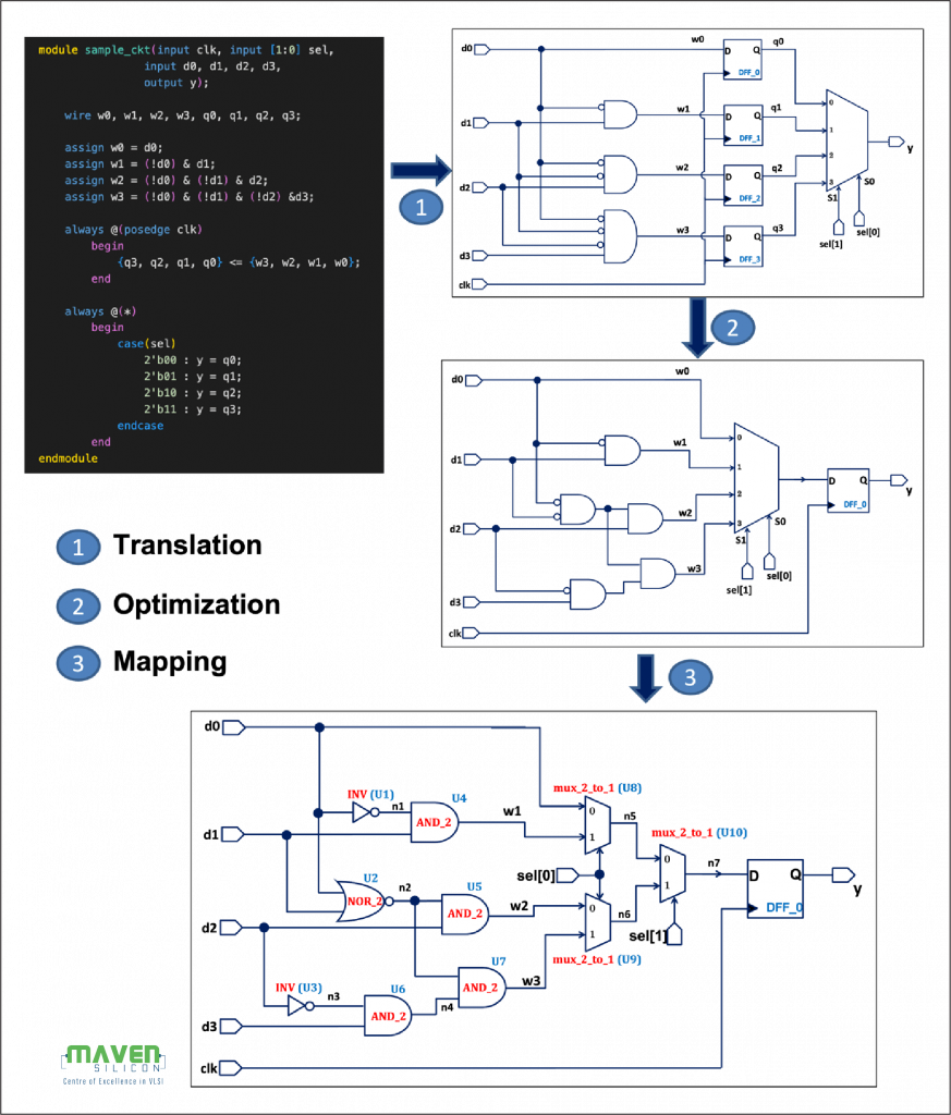

But, this direct translation uses 4 no. of D flip-flops and some logic gates with large fan-in like 4. Gates with larger fan-in are quite bigger in size and slower in operation. So, the synthesis tools will try to optimize the netlist as shown in step 2. Now, the optimized netlist requires only 1 flipflop and gates with a smaller fan-in as opposed to the netlist in the translation stage.
During the optimization, the synthesis tool will also try to reuse some of the partial outputs (for example – the partial output, (!d0 & !d1) is reused for deriving both w2 and w3). This kind of reuse makes the whole gate level netlist with minimum gate count (lesser gate count implies lesser power consumption) and with a better speed.
Similarly, during the mapping stage (Step 3), the synthesis tool will map the logic blocks available in the optimized netlist, with the equivalent logic cells available in the library depending upon the requirements such as power, area, and speed as discussed earlier and generate an updated gate level netlist with the mapped cells from the library. If the standard cell library does not contain some specific blocks that are there in the optimized netlist, then the Synthesis tool will try to implement these blocks using the cells available in the standard cell library. For example, in the optimized netlist, there was a 4:1 Multiplexer and if the standard cell library doesn’t contain a 4:1 Multiplexer, then, the synthesis tool tries to implement it using 2:1 Multiplexers available in the standard cell library as shown in the above picture. Similarly, the library may not contain AND gate with inverted inputs which is there in the optimized netlist in step 2. So, the Synthesis tool will replace it with an equivalent 2-input NOR gate (U2) available in the library.
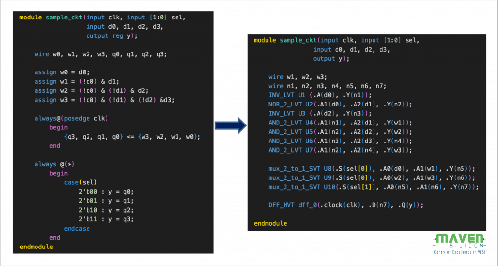
As you can observe in a sample Gate Level Netlist below, Synthesis Tool can use logic cells from different libraries with different characteristics such as LVT, HVT, and SVT depending on the area of the chip, speed required, and maximum amount of power consumption which are defined with the help of various constraints.

Finally, as a result of the synthesis process, the following files will be generated as results along with timing and area reports.
- Gate Level Netlist in Verilog HDL.
- Final SDC: The constraint file with some additional constraints based on the logic cells chosen while doing synthesis. This will be an input constraint file for the implementation tool (For Placement and Routing) for estimating power and timing more accurately.
- .def file: This netlist file contains the initial floor-planning and placement-related data which will be used by the P&R tool to continue to do floor-planning and placement more precisely.
In this article, I have shared my insights into the Physical Synthesis process. If you are interested in starting your career in VLSI Physical Design, you can learn and gain hands-on experience with Synopsys and Siemens EDA tools from our Maven Silicon Advanced Physical Design & Verification Course.