
Global semiconductor industry’s yearly revenue in 2018 was $476.7 Billion. Semiconductor industry includes different kinds of companies like Chip Makers – ASIC & FPGA, Fabless-IP, EDA [Electronic Design Automation], Design Services, PCB Design, Foundry, etc.
Chip Makers create chips using either Application Specific Integrated Circuit [ASIC] or Field Programmable Gate Arrays [FPGAs]. Companies use ASICs work with foundries to fabricate their chips whereas FPGA solution providers buy FPGAs and configure them with their design. In order to design the chip, they need to create in-house IPs or buy external IPs from the fabless Intellectual Property [IP] providers. Also, they need EDA tools like simulators, Synthesizers and P&R to design the IPs.
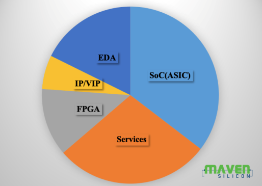

EDA companies like Mentor Graphics, Synopsys, and Cadence provide EDA tools. Design services companies like Wipro, TCS, Altran, etc. provide engineers as consultants to the chip makers. Chip/IP Makers, EDA Companies and Design Services companies together form the VLSI design ecosystem. Also, foundries like TSMC, Global Foundry, etc fabricate the chips & SoCs created by the chip makers.
Samsung, Intel, TSMC, SK Hynix, Micron, Broadcom, Qualcomm, Toshiba, TI, Nvidia, etc are some of the largest semiconductor companies in the world. The United States, Germany, South Korea, Taiwan, Japan, Germany, China, Israel and Singapore are some of the countries which are majorly into semiconductor business. Countries like Switzerland, Netherlands and India are also part of the semiconductor industry ecosystem worldwide.
Product companies that create chips or IPs can be classified based on their domain expertise as:
Processor – Intel, AMD, ARM, Nvidia, SiFi
Wireless – Qualcomm, Broadcom
Automotive – NXP, Infineon, Analog Devices
Memory – Micron, Rambus, Sandisk
Mobile SoC – Apple, Samsung
Indian Semiconductor Ecosystem:
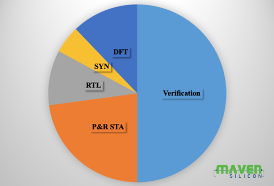
In India, we are majorly into VLSI design services, while providing the other offerings like FPGA based solutions, fabless IP design, PCB design, etc. to the semiconductor industry worldwide. As shown in the figure, chip verification and back-end implementation are the major part of the design services that includes various other services like DFT, RTL, Syn, Analog Design, Testing, Validation, FPGA prototyping, etc.

We engineers are highly skilled in VLSI design and verification, as we are usually well known as skilled software programmers to the world. Our VLSI design skill and domain expertise are in high demand for the global semiconductor companies to create high quality complex chips and SoCs. So, naturally India emerges as a hub that provides highly skilled VLSI engineers to the semiconductor ecosystem worldwide.