
With the continuous and enormous increase in the complexity of modern-day chips, it is almost impossible for any chipmaker/IDM company to design an SoC from scratch. So, these chipmakers will depend on other IP (Intellectual Property) development companies for some of the sub-blocks and they will design the remaining sub-blocks on their own, for designing the complex SoCs as shown in the below figure. Using SoC design methodology, we integrate almost all these components/sub-blocks on a single die and fabricate it as a chip. To understand more about SoC, I recommend the readers, to go through the article on SoC.
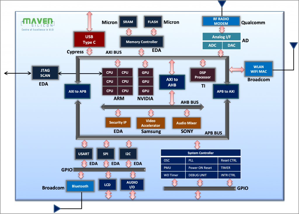

Fig.1.1
The IPs that will be used while designing SoCs, will be available in different forms such as Soft macros, Firm macros, and Hard macros. Soft macros are the designs available in Synthesizable RTL form. Soft macros are not specific to any specific manufacturing process and are not targeted to any specific standard cell library. So, they offer more flexibility.
Firm macros are the designs available in the Gate Level Netlist form targeted to a specific library. During the design process of Firm Macros, they will be optimized for speed, power, and area. They are less flexible than soft macros and more flexible when compared with hard macros, since, the floorplan, placement, and routing within a firm macro can be customized by the designer.
Hard macros are generally available in GDS-II format which means the floorplan, placement, CTS, and routing are already done for these designs and they can be directly used as sub-blocks while designing the top-level SoC. So, they don’t offer much flexibility other than changing the orientation or changing the position and we can’t modify anything within a hard macro apart from accessing the I/O ports. Examples of hard macros are memories and MP4 decoders etc, since they offer a single functionality. They would have been optimized for speed, power, and area already.
Designing complex chips such as SoCs with several IPs and our custom designs involves several processes as explained in the article on Physical Design Flow. In my previous article on Practical Physical Synthesis, I have tried to explain the practical physical synthesis process in detail, and in this article, I will try to cover Placement & Routing processes in detail. Placement & Routing are very important steps in the design flow for achieving a compact, high-performance, and manufacturable chip design.
During the physical synthesis process, the synthesis tools will generate the gate-level netlist along with an initial floorplan for the Silicon chip to minimize multiple iterations between P&R flow (Placement & Routing flow) and Synthesis. During the initial floor-planning phase, the synthesis tool will determine the space for the I/O pins of the chip, position for hard macros, decide the power network, and the remaining area of the silicon chip will be dedicated for placing the standard cells corresponding to the synthesized netlist.
So, during the placement stage, the P&R tool will determine the suitable location for all the standard cells on the floor area of the silicon chip. So, the objective of the placement process is, to find the optimal location of the standard cells that minimizes the area of the chip, power consumption, and signal delays while meeting the design constraints and satisfying the Design Rules. Overall QoR (Quality of Results) of the design greatly depends upon how well, the placement is done, because, based on the way, in which the placement is done, the following parameters will be affected.
- Interconnecting wire length and wire delays.
- Congestion in the routing network.
- Power consumption of the chip.
- Heat distribution across the chip.
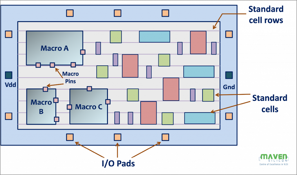

Fig.1.2
Once the placement is completed, the location of various standard cells will be fixed as shown in the above figure. Once the placement is completed, Clock Tree Synthesis (CTS) will be performed on the design to ensure that, the clock is distributed to various flipflops in the design with a minimum amount of clock skew. I will discuss about CTS process in detail in another article.
In the design flow, the subsequent process after completion of CTS is Routing. It involves connecting various standard cells and macros using the interconnecting wires to establish connectivity for achieving the required functionality. The objectives of routing are listed below.
- Minimizing wire length: It will have an impact on reducing the wire delays which will improve the overall performance of the design.
- Minimizing the congestion hotspots: Minimizing the congestion will help us to ensure that, signal integrity is maintained.
Various inputs required for the Physical Implementation (P&R) tool for performing placement, CTS, and Routing are
- Gate Level Netlist
- Initial Floorplan (.def)
- Libraries Used for Synthesis
- Design Constraints (SDC)
- Initial floorplan constraints.
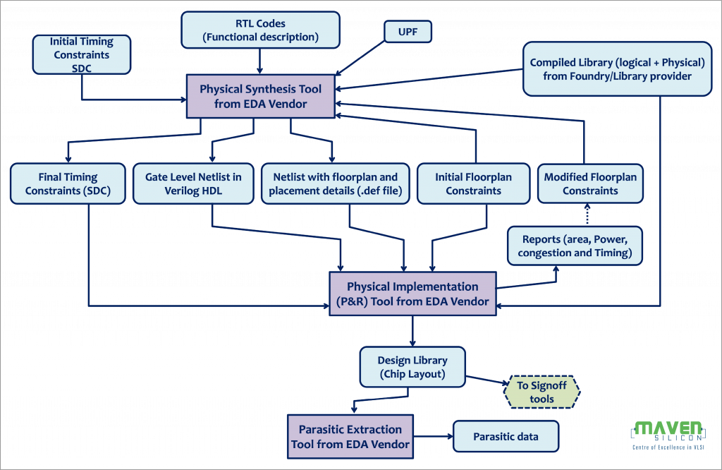

Fig.1.3
As shown in the above figure, the Gate Level Netlist, the initial floorplan, and the design constraints (SDC) will be derived from the Synthesis Process and additional constraints can be added, if required. After the completion of the Synthesis, the P&R tool itself can perform placement, CTS, routing, optimization, and initial level Timing checks as well. If the timing requirements and other design constraints are not satisfied, the P&R tool will optimize the design to ensure that, all the constraints are satisfied. If the area, power, timing, and congestion reports generated by the P&R tool are not satisfactory or the timing requirements or other design constraints such as area and power are not satisfied, after all the possible optimizations during the P&R Processes, then, we may need to go back to Synthesis for further optimization by imposing additional floor-planning constraints to the Synthesis tool.
After the successful completion of placement and routing processes, we will be able to generate the design library which contains the manufacturable layout (GDS-II). This GDS-II file can be used for signoff (Physical Verification) and the design library can be used for parasitic extraction by a dedicated Parasitic Extraction tool from EDA. The extracted parasitic information will be used to perform Timing Analysis in the later stages.
In this article, I have given an overview of the Practical P&R Flow. If you are more interested in starting your career in VLSI Physical Design, you can learn and gain hands-on experience with Synopsys and Siemens EDA tools from our Advanced Physical Design & Verification Course.