Executive Certification in VLSI Design for Testing
With 100% Placement Assistance *
Where Elite Learning Fuels Elite Careers.

A proven track record
Years of Excellence
Years avg exp. of expert faculties
Industry Partners
Active Learners
About iHUB DivyaSampark, IIT Roorkee
iHUB DivyaSampark is a Section 8, not-for-profit Technology Innovation Hub at IIT Roorkee, established under the National Mission on Interdisciplinary Cyber-Physical Systems (NM-ICPS) by the Department of Science & Technology (DST), Government of India.
The hub is dedicated to fostering innovation in emerging technologies such as Artificial Intelligence, Machine Learning, Drones, Robotics, and Data Analytics, collectively known as Cyber-Physical Systems (CPS). iHUB aims to become a key enabler of next-generation digital products, services, and solutions across strategic national sectors including healthcare, Industry 4.0, smart cities, and defense.
Coordinated by a high-level inter-ministerial committee chaired by the CEO of NITI Aayog, and senior officials from DST, MeitY, and other ministries, iHUB DivyaSampark works to create an innovation-driven ecosystem by connecting researchers, entrepreneurs, industry, and academia.
Our Faculties

Sumit Mohanty
Technical Lead
13+ Years
Embedded System

Hemachandra Ramanath Bhat
Chief Technical Officer
37+ Years
Computer Architecture, SoC Design, Embedded Systems Design

Shaik Rafi Ahamed
Professor
20+ Years
Department of Electronics and Electrical Engineering, IIT Guwahati

Mr. Gaurav Trivedi
Program Coordinator and Expert
19+ Years
Department of Electronics and Electrical Engineering, IIT Guwahati

Sinduja K
Head - Technical Training
12+ Years
ASIC Verification

Dr Chiranjeevi G N
Senior Member Technical Staff
14+ Years
VLSI, PD

Basavaraj H
Technical Lead
11+ Years
Advanced Digital Design & RTL Design

Raghavendra Havaldar
Senior Member Technical Staff
18+ Years
RTL Design
Sumit Mohanty
Technical Lead
13+ Years
Embedded System
Hemachandra Ramanath Bhat
Chief Technical Officer
37+ Years
Computer Architecture, SoC Design, Embedded Systems Design
Program Highlights


About the Executive Certification in VLSI Design for Testing
In the AI era, chip designers are empowered with AI-powered EDA tools, silicon-proven IP libraries, and open computing platforms like RISC-V, enabling the efficient design of powerful SoCs for next-generation products. However, ensuring testability and fault coverage is equally critical for first-pass silicon success. This is the right time for chip designers and VLSI enthusiasts to explore ASIC Design for Testing (DFT) methodologies—covering scan insertion, ATPG, fault modeling, BIST, boundary scan, JTAG, and advanced techniques for low-power and high-performance designs. A strong foundation in DFT ensures high-quality, reliable SoCs ready for mass production.
This course provides a comprehensive foundation in Design For Testing. Learners begin with an overview of VLSI, Moore’s Law, SoC architecture, and design flows, followed by digital logic fundamentals such as number systems, combinational and sequential circuits, FSMs, and memory design. The course advances into practical hardware design and verification using Verilog HDL programming - coding styles, FSM design, and lab exercises. It then walks you through CMOS fundamentals, Synthesis, Clock Domain Crossing, STA, Equivalence Checking, and Physical Design Flow - floor planning, placement, CTS, routing, layout compaction, and physical verification (DRC, LVS, IR drop, EM), with labs and case studies.
The Design For Testing module covers verification vs testing, scan insertion, ATPG, fault modelling, BIST, boundary Scan, Test compression, DRC & Test coverage, JTAG, DFT for Analog Macros, while automation skills are developed with Tcl and Python scripting. Students also learn version control with Git, before progressing to advanced DFT concepts and doing an industry standard project – DFT implementation on an SoC.


What Makes This Exclusive Collaboration a Benchmark in Learning Excellence?

Highly Rated Courses
Curriculum crafted and regularly updated by top semiconductor professionals, aligned with job market needs.

Superior Training Methodology and Infrastructure
Self-paced and live online classes with Q&A, featuring 70% hands-on learning through labs, mini-projects, and a final capstone project.

Course Completion Certificate
Earn an iHUB DivyaSampark,IIT Roorkee certified credential recognized by the semiconductor industry and showcase your verified skills to employers and recruiters worldwide.

Industry-Oriented Project
Solve real-world challenges with 24/7 lab and EDA tool access, and enhance your portfolio through impactful, project-based learning.

Value for Money
Get exceptional value for your investment with our budget-friendly offerings.

Masterclasses by IIT Faculty or Industry Experts
Exclusive masterclasses offering cutting-edge insights, real-world case studies, and advanced techniques to elevate your VLSI and Embedded Systems expertise.
Admission Process
The application process comprises three steps. Candidates are required to submit their application. Selected candidates will receive an offer of admission, which must be confirmed by paying the admission fee.
 SUBMIT APPLICATION
- APPLICATION REVIEW & INTERVIEW
- ADMISSION LETTER


Executive Certification in VLSI Design for Testing
Upcoming Program Cohorts
| # | Start Date | Price | Placement Support | |
|---|---|---|---|---|
| 1 | 28th February | 2,00,000 | Job Assistance | 15 Seats Left |
Choose Your Career Track
Take your career in VLSI to the next level with our Executive Certification in ASIC Verification
| # | Course | Duration | Price |
|---|---|---|---|
| 1 | Executive Certification in VLSI Design for Testing With Placement * | 9 Months | ₹2,00,000 + GST |
Price: ₹2,00,000 + GST
Duration: 9 Months
Candidates can pay for the courses through


Share your details to get expert guidance and get eligible for 40% scholarship.
Share your details to get expert guidance and get eligible for 40% scholarship.
Explore our other Executive Certification Courses


Executive Post Graduate Certification in VLSI SoC Design and Verification
- VLSI SoC Design
- SoC Design - Methodology, Process & Fabrication
- ARM and RISC-V Processor Architecture
- SoC protocols: AMBA, I2C, SPI, UART, GPIO
- Advanced SoC: Chiplets, UCIe, Multi-Die Systems
- Software: OS, Firmware, Device Drivers, Toolchain
- Theory, Labs & Project


Our Industry
Partners

* Logos are the trademarks of the respective organizations.
Still not ready?
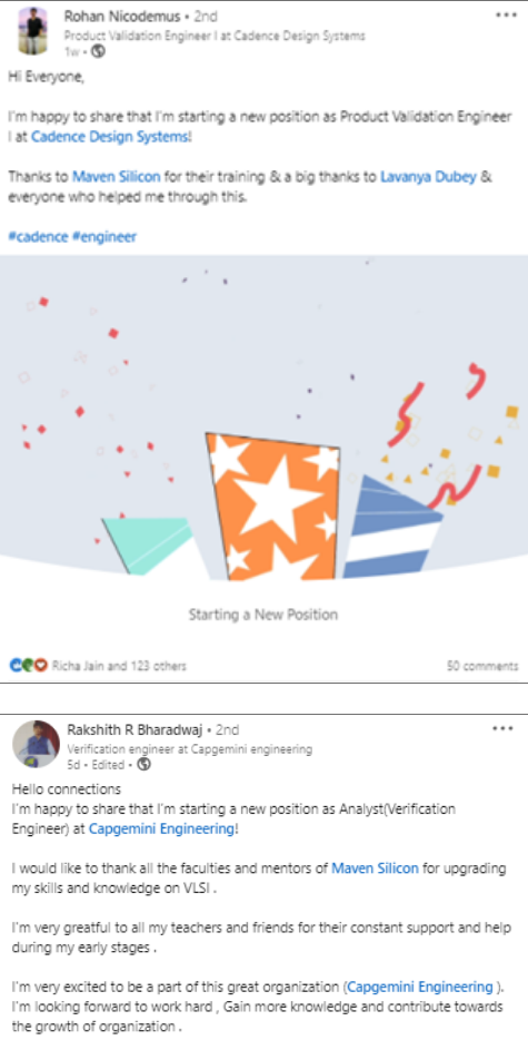
Listen to Our Trainees