


Dynamic Course Structure Designed And Delivered by Industry Experts
Physical Design Internship
Why Choose the Maven Silicon Physical Design Internship?

Student Review
With this internship I am quite confident that I have learnt the basic for creating an VLSI system.

Hardik.S
SSMRV Degree College
I have completed the Embedded System Design Internship at Maven Silicon, where I had the opportunity to work on real-time projects. The internship was very effective and helped me gain hands-on experience.

Lakkakula Deepthi
Narayana Engineering College,Gudur
I had a great experience during the internship. I also improved my understanding of embedded systems concepts, which has been very valuable for my career development

Patel Mann Piyushkumar
Ldrp institute of research and technical
This internship is really developed me in embedded domain, and this certification will make my resume with good weightage.

Gunisetti Tarakeswara rao
Rajiv gandhi university of knowledge technologies
With this internship I am quite confident that I have learnt the basic for creating an VLSI system.
Hardik.S
SSMRV Degree College
I have completed the Embedded System Design Internship at Maven Silicon, where I had the opportunity to work on real-time projects. The internship was very effective and helped me gain hands-on experience.
Lakkakula Deepthi
Narayana Engineering College,Gudur
I had a great experience during the internship. I also improved my understanding of embedded systems concepts, which has been very valuable for my career development
Patel Mann Piyushkumar
Ldrp institute of research and technical
This internship is really developed me in embedded domain, and this certification will make my resume with good weightage.
Gunisetti Tarakeswara rao
Rajiv gandhi university of knowledge technologies
Features

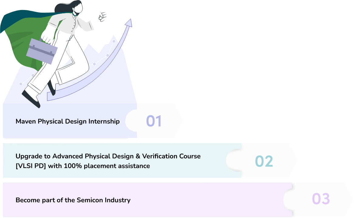
Free Online Foundation - Physical Design course FREE

Upgrade to Advanced Physical Design & Verification Course [VLSI PD] with 100% placement assistance EASY UPGRADE

Internship Certificate from Aceic Design Technologies Pvt Ltd.

24/7 Lab Access and support

Inexpensive VLSI Course

Well Defined Labs and Industry Standard Projects
Course Delivered by Industry Experts

About Internship
Physical Design Internship
This course provides a comprehensive journey into VLSI Physical Design, focusing on the complete back-end flow from RTL to GDSII. Students learn core methodologies, including floorplanning, power planning, placement, clock tree synthesis, routing, and optimization, along with advanced topics such as static timing analysis, signal integrity, IR drop, and electromigration to ensure performance and reliability. The curriculum also introduces design for testability (DFT) integration and Physical Verification Flows (DRC, LVS, ERC) for layout validation. Through hands-on labs with industry-standard tools, learners gain practical skills in timing closure, area/power optimization, and congestion management. The course culminates in a full Physical Design Project, preparing students for professional roles in semiconductor and SoC implementation.
VLSI SoC Design
SoC ASIC Design Flow
Verilog HDL
Linux Operating System
Static Timing Analysis
Floor Planning
Placement
Routing
Design for Testability [ DFT ]
Physical Verification - Overview
Industry Standard Project


Who Can Apply?
This physical design internship is ideal for:
Batch Calendar
Physical Design Internship [PDI]
REGISTRATION OPEN

Physical Design Internship [PDI]
REGISTRATION OPEN
Maven's Placements
5000+
Total placed
250+
Recruiters


Maven Silicon is not like other institutes. I have searched a lot for many VLSI industries at last I joined Maven silicon. It is the best place to get good training and lab facilities and exams to get skilled in the VLSI domain. Within 4 months, I got an early placement opportunity and got placed in L&T.


Recently I got a placement in Truechip solutions even before the completion of the course. The trainers, faculties, and mentors are very helpful and provide us with crystal clear concepts. I am thankful to the whole Maven silicon team and I recommend it for all those who want to pursue their career in the VLSI industry.


My time at Maven silicon was an experience I will cherish forever. The internship has given me wonderful hands-on experience on live projects which will help me in my career. The friendly attitude of the trainers and their willingness to always offer a helping hand have made me feel a part of their family.


Obviously Maven Silicon is the best VLSI training institute. During course the guidance provided by mentors, especially special business communication & language grooming sessions helped me to get placed in Capgemini. I really appreciate the standards set by maven and thankful to each & everyone


Maven Silicon is definitely the best place for all the VLSI aspirants who are interested to carry forward their journey in core VLSI companies. Their training helped me get placed in my dream company i.e. Synopsys. I would like to thank all my mentors from Maven Silicon for taking efforts to make the concepts crystal clear. Apart from this, I would also appreciate the efforts from the technical team and the placement team for providing rigorous efforts to make us all placement-ready.


Maven has the best trainers whether its technical, communication or mentors. Their passion for teaching is astonishing, they are always open to help and ready to support your career, always update with market demands in VLSI. They have the best placement team as well. I could have never achieved my dream without Maven, one of best choice i made in my career by trusting them.


Maven silicon is a very prestigious institute that provides training and placement in the VLSI domain in the best possible way. It is the best place where you can get good training and lab facilities to enhance your knowledge and skills in the VLSI domain. The Placement Support is also very good. They keep you engaged in concept-building activities and give you opportunities till you get placed.

For a non IITian/NITian who finds it difficult to enter VLSI domain, it is the best place to learn skillsets and start a successful career in VLSI domain. The course is well structured and provides VPN access to practise the learnt knowledge remotely on your personal system. The teaching faculty imparts the subject knowledge in an easy to understand way by giving the real life interesting examples and irrespective of the batch size the faculty tries to clear doubts of everyone. Maven provides ample of amazing placement opportunites which includes big dream product as well service based companies.


The Job Oriented Course structure of Advanced VLSI Design and Verification at Maven Silicon perfectly suits all the necessary skills required for an individual to enter the VLSI Industry by staying ahead of all the individuals.

I have enrolled myself into job oriented course of Maven Silicon and it became very fruitful for me. As I got placed in cadence. The course is well structured, in course not only you get technical part but also business communication.Which is very helpful to crack an interview. The technical part is more than sufficient to get into VLSI industry. The labs and projects give you a great insight about the Digital VLSI domain.

Maven Silicon is the best VLSI Training Institute as the course is very well structured, and highly experienced faculty conduct Q and A sessions, which clarify our doubts. Mentor sessions and lab facilities help us understand the concept in-depth, and also business communication classes help in personal development. Overall the training and placement facilities are excellent. I am delighted that I got placed in Synopsys.


My time at Maven Silicon as a Design Intern has taught me both professionally and personally. I have been able to expand my skill set and strengthen my skills. My work at Maven Silicon increased my interest in coding. Thank you to my trainers and mentors for their guidance. My internship at Maven Silicon was a worthwhile experience and as a Mavenite I feel that it has prepared me well for my professional career.


The course curriculum is well structured with lots of practical implementations which helped me to crack my interview. In addition to that, the internship was an advantage through which I was able to answer my interview more confidently than before. Thanks to maven silicon for providing me with such a wonderful opportunity that helped me to get my dream job and excel in life.
Maven Silicon is not like other institutes. I have searched a lot for many VLSI industries at last I joined Maven silicon. It is the best place to get good training and lab facilities and exams to get skilled in the VLSI domain. Within 4 months, I got an early placement opportunity and got placed in L&T.
Recently I got a placement in Truechip solutions even before the completion of the course. The trainers, faculties, and mentors are very helpful and provide us with crystal clear concepts. I am thankful to the whole Maven silicon team and I recommend it for all those who want to pursue their career in the VLSI industry.
My time at Maven silicon was an experience I will cherish forever. The internship has given me wonderful hands-on experience on live projects which will help me in my career. The friendly attitude of the trainers and their willingness to always offer a helping hand have made me feel a part of their family.
Obviously Maven Silicon is the best VLSI training institute. During course the guidance provided by mentors, especially special business communication & language grooming sessions helped me to get placed in Capgemini. I really appreciate the standards set by maven and thankful to each & everyone
Maven Silicon is definitely the best place for all the VLSI aspirants who are interested to carry forward their journey in core VLSI companies. Their training helped me get placed in my dream company i.e. Synopsys. I would like to thank all my mentors from Maven Silicon for taking efforts to make the concepts crystal clear. Apart from this, I would also appreciate the efforts from the technical team and the placement team for providing rigorous efforts to make us all placement-ready.
Maven has the best trainers whether its technical, communication or mentors. Their passion for teaching is astonishing, they are always open to help and ready to support your career, always update with market demands in VLSI. They have the best placement team as well. I could have never achieved my dream without Maven, one of best choice i made in my career by trusting them.
Maven silicon is a very prestigious institute that provides training and placement in the VLSI domain in the best possible way. It is the best place where you can get good training and lab facilities to enhance your knowledge and skills in the VLSI domain. The Placement Support is also very good. They keep you engaged in concept-building activities and give you opportunities till you get placed.
For a non IITian/NITian who finds it difficult to enter VLSI domain, it is the best place to learn skillsets and start a successful career in VLSI domain. The course is well structured and provides VPN access to practise the learnt knowledge remotely on your personal system. The teaching faculty imparts the subject knowledge in an easy to understand way by giving the real life interesting examples and irrespective of the batch size the faculty tries to clear doubts of everyone. Maven provides ample of amazing placement opportunites which includes big dream product as well service based companies.
The Job Oriented Course structure of Advanced VLSI Design and Verification at Maven Silicon perfectly suits all the necessary skills required for an individual to enter the VLSI Industry by staying ahead of all the individuals.
I have enrolled myself into job oriented course of Maven Silicon and it became very fruitful for me. As I got placed in cadence. The course is well structured, in course not only you get technical part but also business communication.Which is very helpful to crack an interview. The technical part is more than sufficient to get into VLSI industry. The labs and projects give you a great insight about the Digital VLSI domain.
Maven Silicon is the best VLSI Training Institute as the course is very well structured, and highly experienced faculty conduct Q and A sessions, which clarify our doubts. Mentor sessions and lab facilities help us understand the concept in-depth, and also business communication classes help in personal development. Overall the training and placement facilities are excellent. I am delighted that I got placed in Synopsys.
My time at Maven Silicon as a Design Intern has taught me both professionally and personally. I have been able to expand my skill set and strengthen my skills. My work at Maven Silicon increased my interest in coding. Thank you to my trainers and mentors for their guidance. My internship at Maven Silicon was a worthwhile experience and as a Mavenite I feel that it has prepared me well for my professional career.
The course curriculum is well structured with lots of practical implementations which helped me to crack my interview. In addition to that, the internship was an advantage through which I was able to answer my interview more confidently than before. Thanks to maven silicon for providing me with such a wonderful opportunity that helped me to get my dream job and excel in life.
* Logos are the trademarks of the respective organizations.
Recruiters Review
Good experience through the overall hiring process. Looking forward to a long term engagement.
We have always received good resumes and great talents from Maven.

We really appreciate the way the candidates are performing and would expect them to give their best with excellence every time.

It has been a great experience with the Maven team. We hired around 50+ candidates. It has been a smooth experience to work with the team during the entire process.

Overall Experience in Hiring from the Institute is good. The responses from the placement team are on time and they are very supportive.

Test and interview process was smooth.

The resource quality from Maven is of very high standards and the best in industry. The placement team is also very proactive and supportive.

Overall good candidates compared to regular freshers or from any other institutes. One of the best institutes where you can find candidates from different states with a variety of skill sets. Thanks to maven for all the support.

It was really nice to see freshers with such a quality understanding of the basics of RTL design and verification. Overall recruitment experience was smooth. Looking forward to a long relationship with Maven

Very Supportive & Quick assertiveness
Test and interview process was smooth.

We are truly delighted by the level of commitment and professionalism given by your team. The resources are good at fundamentals and know what the industry demands from them.

We are pleased with the support & coordination by the Maven team, thank you! The quality of applicants from Maven are very good, credits to Maven for their industry relevant course content, teaching staff and of course the applicants.

Overall Experience is very good to hire good resources with the help of an active and supportive team.

The resource quality is excellent. The placement team is always supportive and provides the right fit for our company. I am very confident about the profiles that I receive from Maven.

We had a good experience in hiring freshers for our FPGA role from Maven Silicon. Update from business is they are performing very well in their assigned job roles.

Support from the Placement Team is very good. We always want to work with Maven Silicon.

Overall experience on hiring is good, Maven has quite a good resource pool and it helps to bridge the gap between companies to colleges - where engineers lack the push to enter the VLSI domain. Hiring process to onboarding was smooth and easy

Good candidates with Supportive team
Good experience through the overall hiring process. Looking forward to a long term engagement.
We have always received good resumes and great talents from Maven.
We really appreciate the way the candidates are performing and would expect them to give their best with excellence every time.
It has been a great experience with the Maven team. We hired around 50+ candidates. It has been a smooth experience to work with the team during the entire process.
Overall Experience in Hiring from the Institute is good. The responses from the placement team are on time and they are very supportive.
Test and interview process was smooth.
The resource quality from Maven is of very high standards and the best in industry. The placement team is also very proactive and supportive.
Overall good candidates compared to regular freshers or from any other institutes. One of the best institutes where you can find candidates from different states with a variety of skill sets. Thanks to maven for all the support.
It was really nice to see freshers with such a quality understanding of the basics of RTL design and verification. Overall recruitment experience was smooth. Looking forward to a long relationship with Maven
Very Supportive & Quick assertiveness
Test and interview process was smooth.
We are truly delighted by the level of commitment and professionalism given by your team. The resources are good at fundamentals and know what the industry demands from them.
We are pleased with the support & coordination by the Maven team, thank you! The quality of applicants from Maven are very good, credits to Maven for their industry relevant course content, teaching staff and of course the applicants.
Overall Experience is very good to hire good resources with the help of an active and supportive team.
The resource quality is excellent. The placement team is always supportive and provides the right fit for our company. I am very confident about the profiles that I receive from Maven.
We had a good experience in hiring freshers for our FPGA role from Maven Silicon. Update from business is they are performing very well in their assigned job roles.
Support from the Placement Team is very good. We always want to work with Maven Silicon.
Overall experience on hiring is good, Maven has quite a good resource pool and it helps to bridge the gap between companies to colleges - where engineers lack the push to enter the VLSI domain. Hiring process to onboarding was smooth and easy
Good candidates with Supportive team
* Logos are the trademarks of the respective organizations.
Your Career Path
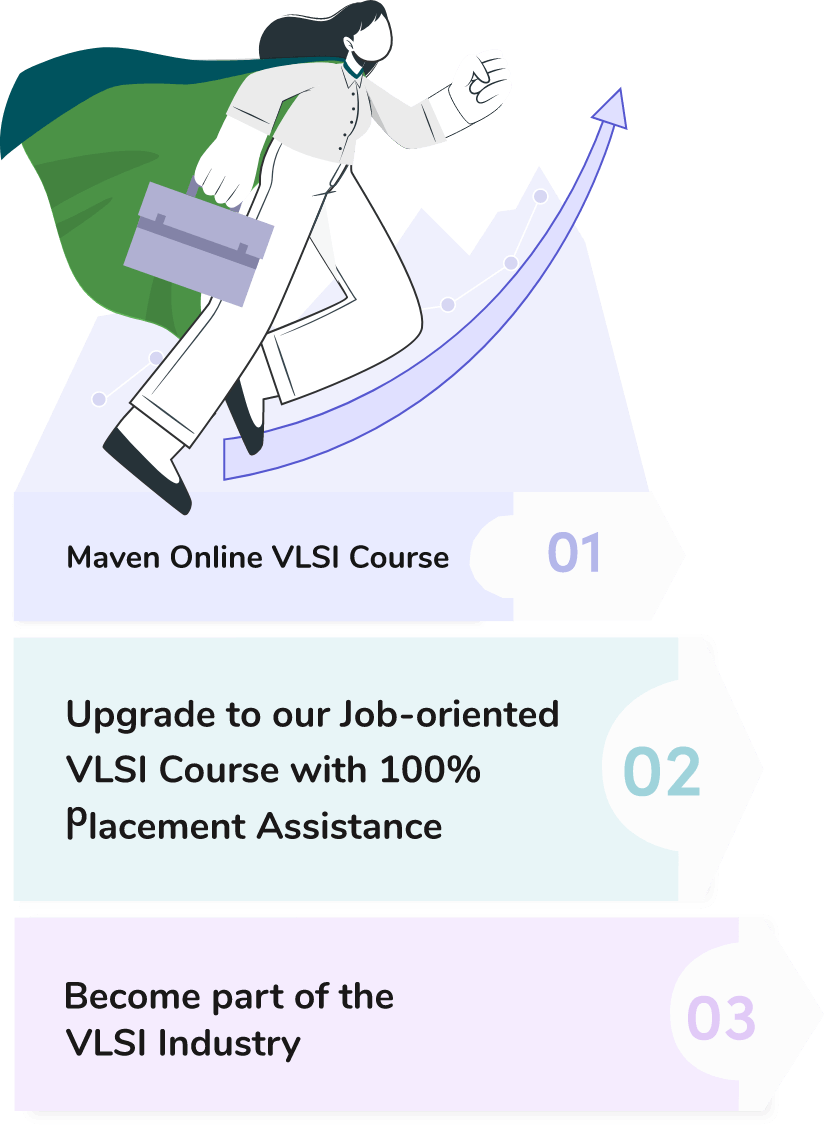
Expand your Semicon Career Opportunities with Maven Silicon
Job-oriented VLSI courses
Online VLSI & Embedded System Courses
Job-oriented Embedded Systems course
VLSI & Embedded Internship
Executive Certification Courses
Executive M.Tech in VLSI Design from PES


40%OFF
40%OFF
On All Courses
