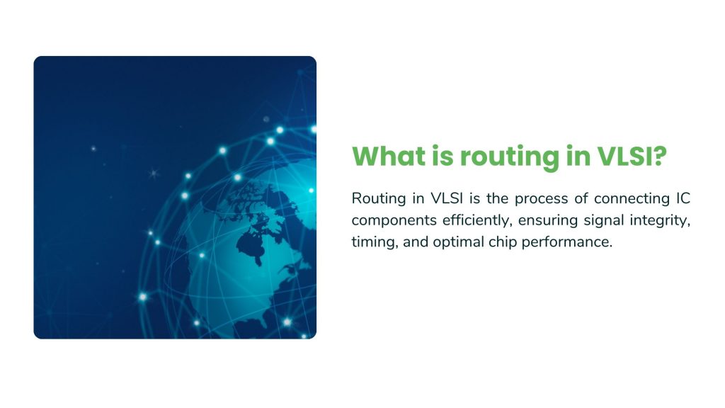
 In the intricate landscape of Very Large Scale Integration (VLSI), the process of “routing” plays a pivotal role in shaping the interconnect design of integrated circuits (ICs). Routing, a fundamental step in VLSI design, involves creating pathways or wiring connections that link various components and modules within the chip.
Understanding Routing in VLSI:
Routing is the meticulous process of planning, designing, and implementing the physical paths that interconnect the numerous logic blocks, memory elements, and other circuit components on the semiconductor chip. These pathways, often represented as metal layers, form the critical infrastructure enabling communication and data transfer between different sections of the IC.
Key Aspects of Routing:
Pathfinding Algorithms:
Sophisticated algorithms are employed to navigate and determine the most optimal and efficient pathways for interconnections. These algorithms consider various factors, including signal timing, signal integrity, power consumption, and area constraints.
Layer Assignment and Metal Stack Planning:
The allocation and organization of interconnections across multiple metal layers involve careful planning to reduce congestion, manage signal propagation delays, and accommodate different routing requirements for different types of signals.
Signal Integrity and Timing Constraints:
Routing aims to ensure signal integrity by minimizing noise, crosstalk, and electromagnetic interference along the routed paths. Adhering to timing constraints is crucial to maintain the synchronization and reliable transmission of signals.
Importance of Routing in VLSI Design:
Efficient routing significantly impacts signal propagation, ensuring that data signals traverse the chip with minimal delays and distortion, ultimately affecting the overall speed and performance of the IC.
Area Utilization and Density Optimization:
Well-optimized routing directly contributes to effective area utilization within the chip layout, allowing for a compact design while accommodating complex interconnections and high circuit density.
Design Closure and Verification:
Successful routing is pivotal for achieving design closure. It involves thorough verification to ensure that the final interconnect design adheres to all design constraints, meets timing requirements, and is ready for fabrication.
Techniques and Best Practices:
Utilizing grid-based or maze-routing techniques to simplify the routing process by organizing interconnections into a grid pattern or navigating through maze-like structures, optimizing pathfinding.
Layer Switching and Via Planning:
Strategically switching between metal layers and planning vias (vertical interconnect access) to efficiently traverse between layers, managing congestion and minimizing signal interference.
Design Rule Checking (DRC) and Design for Manufacturing (DFM):
Conducting rigorous design rule checks (DRC) and design for manufacturing (DFM) analyses to ensure compliance with fabrication constraints and manufacturing requirements during the routing phase.
Conclusion:
Routing stands as a critical phase in VLSI design, influencing the efficiency, reliability, and performance of integrated circuits. Mastery of routing principles, effective utilization of routing strategies, and leveraging advanced routing techniques are indispensable for VLSI engineers to craft high-performance semiconductor devices.