VLSI Industry
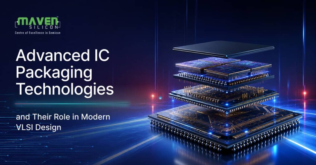
Advanced IC Packaging Technologies and Their Role in Modern VLSI Design
 September 12, 2026
 5 minutes read
 243 Views




Key Takeaways
- Advanced IC packaging is transforming the package from a protective shell into an active part of chip performance.
- Technologies such as 2.5D packaging, 3D ICs, chiplets and fan-out packaging enable greater functionality in smaller spaces.
- Modern packaging can improve performance, bandwidth and power efficiency while creating new thermal and design challenges.
- Understanding integrated circuit packaging is becoming increasingly valuable for VLSI engineers as chip design and package design become more closely connected.
- The future of semiconductor packaging will depend on advanced integration, heterogeneous computing and innovative thermal solutions.
Introduction
Have you ever wondered how a semiconductor device the size of a fingernail can process billions of operations per second whilst managing heat, power and signal integrity without falling apart? If yes, then you have stumbled upon one of the most underappreciated disciplines in modern electronics: integrated circuit packaging.
Most conversations about chip design focus on what happens at the transistor level; gate delays, process nodes, logic synthesis. But packaging is what turns a fragile silicon die into something robust, connectable and commercially viable. Let us unpack it properly.
What is Advanced IC Packaging?
Semiconductor packaging is the process of enclosing a fabricated silicon die within a protective structure that provides electrical connections, mechanical protection, and thermal dissipation.
Advanced IC packaging takes this further by moving beyond simple encapsulation to integrate multiple dies, reduce interconnect distances and enable system-level optimisation that traditional planar scaling alone cannot deliver.
The spectrum of IC chip packaging today is extraordinarily broad, from legacy dual in-line packages (DIP) to cutting-edge 3D stacked structures that vertically integrate memory, logic and analog functions within a single package footprint.
Why Advanced Packaging Matters in Modern VLSI Design?
Transistor scaling alone is no longer enough. As process nodes approach 2nm and below, the returns on purely dimensional shrinking are diminishing whilst costs are escalating sharply. The package is no longer a passive container; it is an active participant in the chip’s electrical performance, power delivery network and thermal envelope.
Key Advanced IC Packaging Technologies
The landscape of various types of IC packages has expanded dramatically in the last decade.
- Flip-Chip BGA (FC-BGA): Solder bumps connect the die face-down directly to the substrate, dramatically shortening interconnect paths compared to wire bonding. Used extensively in CPUs, GPUs and networking chips.
- 2.5D Integration with Silicon Interposers: Multiple dies (logic, HBM memory, SerDes) are mounted side-by-side on a silicon interposer; enabling very short, high-bandwidth interconnects without the yield risk of a monolithic die.
- 3D IC Stacking with TSVs (Through-Silicon Vias): Dies are stacked vertically and connected through silicon vias, delivering the highest bandwidth density and lowest interconnect latency available today.
- Chiplet Architecture: Rather than designing a single large SoC, chiplet-based designs disaggregate functions across multiple smaller dies from potentially different process nodes or foundries, assembled into one package.
- Fan-Out Wafer-Level Packaging (FOWLP): Dies are embedded in a reconstituted wafer with redistribution layers extending connectivity beyond the die boundary; enabling very compact packages without a traditional substrate.
- Package-on-Package (PoP): Stacks logic and memory packages vertically, commonly found in mobile application processors where board space is critical.
Understanding how these package architectures interact with design decisions made during VLSI Design Flow is increasingly essential for engineers at every level of the stack.
Role of Advanced Packaging in Modern VLSI Design
Advanced IC packaging is fundamentally changing design methodology. Package-aware design has emerged as a discipline in its own right; requiring engineers to co-simulate the chip and its package together.
Power delivery networks must now be planned across die and package simultaneously. Thermal management must account for heat generated across stacked dies and dissipated through a shared package structure.
For learners building this broader understanding; Maven Silicon’s online VLSI courses provide exposure to key areas of the VLSI design flow, helping connect design concepts with real industry requirements.
Design Challenges in Advanced IC Packaging
Thermal management is one of the biggest concerns. Closely packed or vertically stacked dies can create concentrated heat and excessive temperature can affect performance and reliability.
Signal and power integrity also become increasingly complex as interconnect density rises. Engineers must carefully manage noise, voltage drops and high-speed signal behaviour.
Then there is testing. When several dies are integrated into one package, identifying where a fault originated can become more challenging.
Maven Silicon’s VLSI Design and Functional Verification programme and Advanced DFT Course help learners build knowledge across important areas of the chip development flow, including design and verification.
Future Trends in Advanced IC Packaging
IC packaging technology will continue to absorb functions that were previously handled by board-level integration or separate chips. Embedded die packaging, photonic integration and chiplet ecosystems with standardised interfaces (UCIe, BoW) will further blur the boundary between chip design and system design.
Skills VLSI Engineers Need for Advanced Packaging
For engineers looking to stay relevant in this evolving landscape, the priority skills include –
- Signal integrity and power integrity co-simulation at the package level
- Thermal analysis tools and methodologies (ANSYS Icepak, FloTHERM)
- Understanding of bump and TSV design rules and their interaction with physical design
- DFT methodology for multi-die systems and heterogeneous integration
- Familiarity with package substrate design and redistribution layer routing
Conclusion
Advanced IC packaging is no longer a downstream concern that chip designers hand off to a packaging team at the end of the process. It is a co-design discipline that shapes performance, power and cost from the earliest architectural decisions through to final product reliability.
That is precisely where Maven Silicon comes in. With over 17 years of delivering industry-aligned VLSI training; including programmes in Physical Design, ASIC Verification, DFT and now Advanced IC Packaging and Manufacturing in collaboration with iHUB IIT Roorkee; Maven Silicon gives you the depth and breadth the industry actually demands.

Share This Post:


75,221
SUBSCRIBERS
Subscribe to our Blog
Get the latest VLSI news, updates, technical and interview resources
