VLSI Industry
From Blocks to Systems: Understanding Chiplets in SoC Design
 September 27, 2025
 4 minutes read
 292 Views


In recent years, the semiconductor industry has witnessed a shift in how complex integrated circuits (ICs) are designed and manufactured. With the growing demand for more powerful, efficient, and modular solutions, chiplets have emerged as a promising alternative to traditional monolithic System-on-Chip (SoC) designs. For someone new to VLSI or physical design, understanding this transition can be overwhelming. This article aims to break it down simply and explain where chiplets fit in the world of SoC design.
What Is a Chiplet?
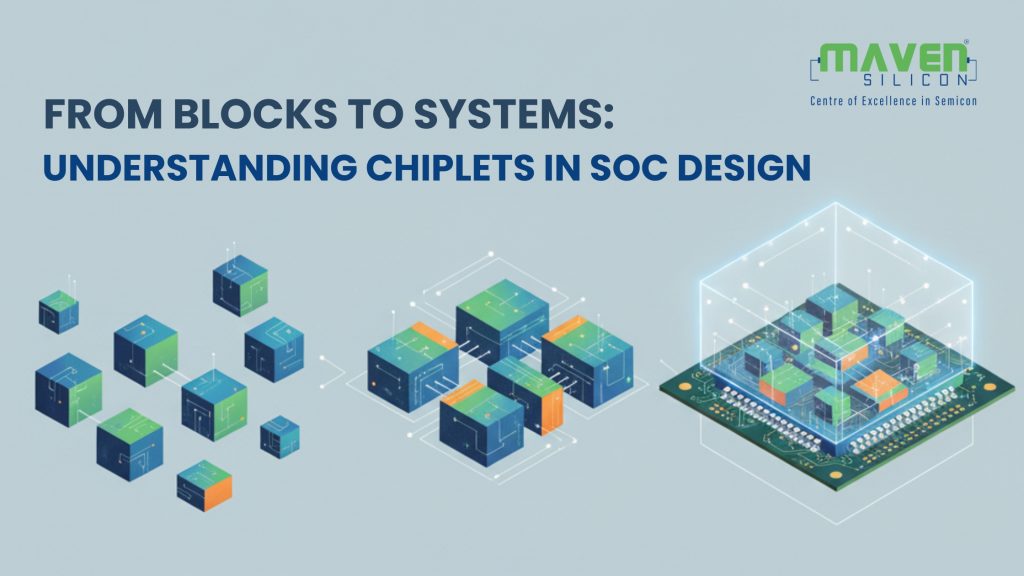
A chiplet is a small functional block of silicon that performs a specific task and can be combined with other chiplets to form a complete system. Think of it like a Lego block that can be connected with others to build a complex structure. Each chiplet may include CPU cores, memory, I/O interfaces, or even specialized accelerators like GPUs or AI engines.
Rather than building an entire SoC as a single die, designers can now disaggregate the system into smaller, reusable chiplets. These chiplets are packaged together using advanced packaging technologies to form a complete, high-performance system.
Why Chiplets?
Here are a few reasons chiplets are gaining popularity:
- Scalability and Modularity: Different chiplets can be reused across multiple products, reducing design time and cost.
- Yield Improvement: Smaller dies are easier to manufacture with fewer defects compared to large monolithic chips.
- Heterogeneous Integration: Chiplets can be fabricated using different process nodes (e.g., 5nm for CPU, 16nm for analog), enabling optimized performance and cost.
- Time to Market: Reusing existing chiplets accelerates the development cycle.
Key Technologies Enabling Chiplets
To connect chiplets efficiently, we rely on advanced packaging techniques like:
- 2.5D and 3D Integration: Uses interposers or stacked dies to connect chiplets.
- Inter-die Communication Standards: Such as UCIe (Universal Chiplet Interconnect Express) or proprietary interfaces.
- High Bandwidth Memory (HBM): Often integrated with compute chiplets in 2.5D packages.
If you’re interested in how 3D ICs are pushing the boundaries of chip design, we have covered this in more detail in our previous blog post on 3D IC Technology.
How Chiplets Fit into SoC Design
Traditionally, SoCs integrate all the functions — CPU, memory, I/O, interconnect — into a single die. In a chiplet-based approach, these functions are split across multiple dies but appear as a single system to software.
Here’s how this shift affects various stages of the design flow:
- Frontend Design: Still involves RTL coding and verification, but now each chiplet might be developed independently.
- Physical Design (PD): The PD team must work with floorplanning, power planning, and timing closure at both the chiplet and package level.
- Package Co-design: Engineers now collaborate closely with packaging teams. Terms like bump planning, RDL (Redistribution Layer), interposer design, and thermal-aware floorplanning become more critical.
- Signal Integrity and Power Integrity (SI/PI): More emphasis is placed on SI/PI analysis due to high-speed links between chiplets.
- DFT (Design for Test): Testing chiplet-based systems can be more complex and requires new strategies for test coverage and test access mechanisms across dies.
Common Physical Design Terms in Context
If you’re stepping into the world of VLSI physical design, here are a few terms you’ll frequently encounter, especially in chiplet-related projects:
- Floorplan: Defining the layout and boundaries of functional blocks (or chiplets) within a die or package.
- Macro placement: Strategically placing large blocks (like memory macros or chiplets) to optimize area and performance.
- Clock Tree Synthesis (CTS): Ensuring that clocks are delivered uniformly across all parts of the chiplet for timing correctness.
- IR Drop: Voltage drop in power lines due to resistance, especially critical when connecting high-power chiplets.
- EM (Electromigration): Reliability concern due to current density in interconnects, a key consideration in chiplet interconnects.
- Routing Congestion: More interfaces between chiplets can lead to congestion, making routing optimization crucial.
Challenges Ahead
While chiplets offer many benefits, they also come with challenges:
- Standardization: The industry still lacks widely accepted standards for chiplet interconnects and packaging.
- Thermal Management: Managing heat across multiple dies packed closely together is not trivial.
- Design Complexity: While modular, chiplet systems add complexity in package-level co-design and verification.
Final Thoughts
The move from monolithic SoCs to chiplet-based systems is a paradigm shift, one that brings exciting opportunities as well as new technical challenges. As technologies like UCIe and 3D packaging mature, chiplets are poised to become a cornerstone of future semiconductor designs.

Share This Post:


75,221
SUBSCRIBERS
Subscribe to our Blog
Get the latest VLSI news, updates, technical and interview resources
