Newsletters
Newsletter July 2026
 July 29, 2026
 8 minutes read
 204 Views




Advancing Semiconductor Excellence Through Workforce Development and Industry Collaboration
The semiconductor industry is entering a new phase of growth, driven by rapid advancements in artificial intelligence, high-performance computing, automotive electronics, and intelligent systems. As technologies continue to evolve, organizations are increasingly investing in developing highly skilled engineering teams capable of designing the next generation of semiconductor solutions.
At Maven Silicon, we remain committed to strengthening the global semiconductor ecosystem by delivering industry-aligned learning programs, enabling large-scale corporate upskilling, fostering strategic collaborations, and engaging with leading industry forums. In this edition of our corporate newsletter, we highlight key initiatives that are empowering engineering professionals, supporting enterprise workforce development, and contributing to the advancement of semiconductor innovation.
AI is Transforming Semiconductor Industry – Upskill Today to Lead Tomorrow
An article by Sivakumar P R, Founder and CEO, Maven Silicon.
The semiconductor industry is evolving at an unprecedented pace as artificial intelligence continues to transform chip design, verification, manufacturing, and system development. Engineers are no longer expected to possess only strong technical fundamentals. They must continuously expand their expertise to keep pace with emerging technologies, advanced design methodologies, and increasingly complex semiconductor systems.
This article explores why continuous upskilling has become essential for engineers seeking long-term career growth in the semiconductor industry. It highlights how organizations can build future-ready engineering teams by investing in structured learning and how professionals can strengthen their technical expertise to remain competitive in an AI-driven semiconductor landscape.
Key perspectives covered include:
- The growing impact of AI on semiconductor design and engineering workflows
- Why continuous learning is becoming essential for engineering professionals
- Building expertise in emerging semiconductor technologies
- Preparing engineers for evolving roles across the semiconductor value chain
- Creating a future-ready workforce through structured industry learning
As semiconductor technologies continue to advance, engineers who invest in continuous learning today will be better positioned to lead tomorrow’s innovations.
Explore the Full Article: AI is Transforming Semiconductor Industry – Upskill Today to Lead Tomorrow
Strengthening Enterprise Workforce Development
Large Scale Corporate Training Initiative
We are proud to partner with a leading global professional services organization to deliver comprehensive semiconductor training for 200 engineers worldwide over the next two years.
The engagement has been designed to strengthen engineering capabilities across four critical semiconductor domains, RTL Design, Design Verification, Design for Testability (DFT), and Physical Design. Through structured learning pathways, hands-on laboratory sessions, and industry-oriented projects, engineers will gain practical expertise aligned with modern semiconductor development practices.
This collaboration reflects the growing importance of continuous workforce development as organizations prepare engineering teams to address increasingly complex semiconductor design challenges. By combining technical depth with practical application, the program will enable engineers to contribute more effectively across the semiconductor design lifecycle while supporting long-term organizational capability development.
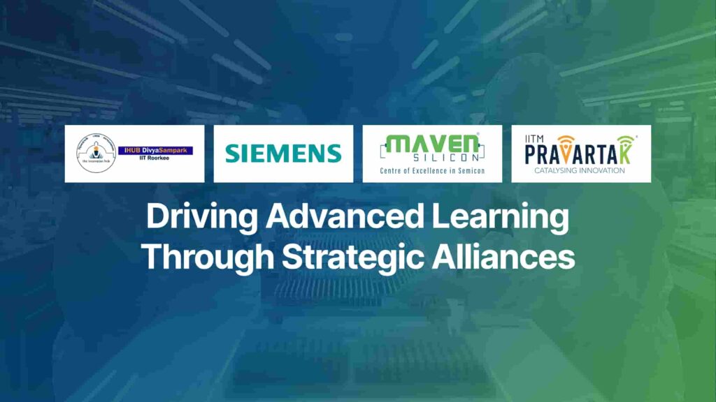
Advancing Professional Learning Through Premier Collaborations
Strategic Collaborations with iHUB DivyaSampark, IIT Roorkee, Siemens and IITM Pravartak
Maven Silicon continues to strengthen professional learning opportunities through collaborations with leading academic and industry institutions, enabling engineers to build expertise in emerging semiconductor technologies.
The Advanced Certification in IC Packaging & Manufacturing, launched in collaboration with iHUB DivyaSampark, IIT Roorkee, and Siemens, addresses the growing demand for advanced skills in semiconductor packaging, manufacturing, chiplet integration, and next generation packaging technologies. The program combines expert-led instruction, industry masterclasses, hands-on learning, campus immersion, and an industry-aligned capstone project to deliver a comprehensive learning experience for engineering professionals.
Further strengthening our commitment to semiconductor workforce development, our strategic alliance with IITM Pravartak offers Professional Certification Programs in VLSI Design and Verification and Embedded Systems Design. These programs provide engineers with access to industry-grade tools, hands-on laboratories, practical projects, faculty interaction, and a campus immersion experience at IIT Madras, enabling participants to develop advanced technical expertise aligned with current industry requirements.
Together, these collaborations provide structured learning pathways that combine academic excellence with practical application, empowering professionals to build future-ready semiconductor expertise and accelerate their careers.
Watch Event Highlights: Launch of the Advanced Certification in IC Packaging & Manufacturing
Read Article: ANI Coverage
Read Article: Education Times
Strengthening Strategic Partnerships Across the Global Semiconductor Ecosystem
Expanding Industry Collaboration
Strategic partnerships continue to play an important role in advancing semiconductor innovation, workforce development, and knowledge sharing across the global industry.
As a proud member of SEMI, Maven Silicon is strengthening its engagement with the international semiconductor community while contributing to discussions on workforce development, emerging technologies, manufacturing, and industry collaboration. This membership enables us to remain aligned with global semiconductor trends while bringing international best practices into our learning ecosystem.
Further strengthening our global industry engagement, our FPGA Training Program is now featured on the Altera Training Calendar, providing engineers and organizations with greater access to specialized learning opportunities in FPGA design and development. The program delivers structured, industry-aligned training covering FPGA architecture, RTL design, verification, implementation, and hands-on development using leading FPGA technologies. This milestone expands the visibility of our professional learning offerings while enabling engineering professionals to build practical expertise that supports innovation across the semiconductor ecosystem.
These collaborations reinforce our commitment to building globally relevant learning experiences while strengthening connections across the semiconductor ecosystem.
Know More: Partnership with SEMI as a Proud Member
Industry Engagement and Conferences
Contributing to the Semiconductor Community
Active participation in industry forums enables meaningful collaboration, knowledge exchange, and stronger engagement with stakeholders across the semiconductor ecosystem. Such engagements help us stay aligned with evolving industry trends, strengthen partnerships with academia and industry, and contribute to the advancement of semiconductor technologies.
During this quarter, Maven Silicon participated in the IESA Members Meet, joining industry leaders, technology experts, and ecosystem partners to discuss innovation, policy initiatives, talent development, and collaborative efforts aimed at strengthening India’s semiconductor ecosystem. The event provided an excellent platform to exchange ideas, understand emerging industry priorities, and engage in discussions on accelerating semiconductor research, design, and workforce development.
As India’s semiconductor landscape continues to evolve, Maven Silicon remains committed to actively participating in industry forums, conferences, and collaborative initiatives that foster innovation, encourage knowledge sharing, and support the development of a highly skilled semiconductor workforce. Through these engagements, we continue to strengthen our relationships with industry stakeholders while contributing to the growth and success of the global semiconductor ecosystem.
Looking Ahead: Building a Future Ready Semiconductor Workforce
As semiconductor technologies continue to transform industries worldwide, the need for highly skilled engineering talent continues to grow. Continuous learning, strategic collaboration, and practical industry experience will remain essential in preparing professionals to address future technology challenges.
Maven Silicon remains committed to empowering engineers through advanced learning programs, enterprise training initiatives, and strategic collaborations with leading academic institutions, industry organizations, and global technology partners. Together, we will continue strengthening the semiconductor talent ecosystem and enabling the next generation of innovation.
Advancing Professional Excellence Through Flagship Programs
To equip professionals with specialized expertise and leadership readiness in the semiconductor domain, Maven Silicon offers advanced, industry-aligned programs in collaboration with top-tier institutions:
iHUB DivyaSampark, IIT Roorkee Executive Certification Programs: These programs focus on cutting-edge VLSI technologies and their real-world applications, designed to elevate professionals into experts in semiconductor design and implementation.
Executive MTech in VLSI Design: Designed for working professionals, this degree program, in collaboration with PES University, provides deep design expertise, system-level thinking, and the tools for accelerating careers in the fast-evolving semiconductor industry.
Advanced Certification in IC Packaging & Manufacturing: This certification, in collaboration with iHUB DivyaSampark, IIT Roorkee and Siemens, is crafted to address the growing demand for specialized skills in semiconductor packaging and manufacturing. It covers advanced packaging techniques, chip assembly, and testing, enabling readiness to contribute to the development of next-generation semiconductors in the AI-driven era.
IITM Pravartak Professional Certification Program: The Professional Certification Program in VLSI Design & Verification and Embedded System Design is designed to enhance advanced skills in VLSI design, verification methodologies, and embedded systems. The program aligns with industry requirements, enabling professionals to strengthen their expertise and progress in VLSI and embedded systems roles.
CREST, BITS Pilani Certification Program: The Certification Program in SystemVerilog for Verification builds advanced expertise in SystemVerilog-based verification methodologies. It focuses on developing robust, scalable, and industry-standard testbenches for complex VLSI designs, aligned with current industry practices for roles in VLSI design and verification.
These programs are designed to foster cutting-edge skills and prepare professionals for leadership roles in the semiconductor industry, with a focus on real-world applicability and future-proofing their careers.
Stay Connected with Maven Silicon
For more information about our professional certification programs, corporate training solutions, and strategic collaborations
Email: enterprise@maven-silicon.com
Website: www.maven-silicon.com/enterprise
Let us continue driving the future of semiconductor innovation through continuous learning, strategic partnerships, and engineering excellence.

Share This Post:


75,221
SUBSCRIBERS
Subscribe to our Blog
Get the latest VLSI news, updates, technical and interview resources
