VLSI Industry
Understanding the Role of Chiplets in Semiconductor Design: A Modular Approach
 September 17, 2026
 9 minutes read
 251 Views




Table of Contents
- Why Are Chiplets Becoming Attractive?
- What Are Chiplets and How Do They Work?
- Why Is the Industry Moving Toward Chiplets?
- Which Wins: Chiplets or Traditional SoC Design?
- What Is India’s Role in the Chiplet Ecosystem?
- Where Are the Opportunities for Engineers in Chiplet Design?
- Which Skills Do You Need to Work with Chiplet Technology?
- What Does the Future Hold: 2026 and Beyond?
- Where Do You Go From Here? Conclusion and Next Steps
Key Takeaways
- Chiplets split a large die into smaller, specialised blocks joined through advanced packaging, lowering cost and improving yield.
- The global chiplet market is growing at a blistering pace, fuelled by AI, HPC, and mobile demand.
- India is emerging as a genuine contender in chip design, backed by government-led semiconductor missions.
- Engineers skilled in packaging, interconnects, and verification are increasingly sought after.
- Chiplets do not replace traditional SoC design; they complement it for specific, high-value use cases.
Why Are Chiplets Becoming Attractive?
For decades, chip designers etched everything onto a single slab of silicon and called it done. That worked well while transistors kept shrinking on schedule. But as process nodes push toward 3nm and below, fabricating one giant die has grown expensive, and a single defect can now ruin an entire chip.
The global semiconductor industry felt this pressure first in high-performance computing and AI accelerators. According to MarketsandMarkets, the global chiplet market is set to grow from USD 51.94 billion in 2025 to USD 157.23 billion by 2030, at a CAGR of 24.8 percent, which signals real industry confidence.
What Are Chiplets and How Do They Work?
Think of a chiplet as a functional silicon die implementing one or more closely related subsystems — say a CPU core, a memory controller, or an I/O block — and gets wired together with other bricks inside a single package. Instead of building one enormous monolithic die, engineers now assemble a chiplet architecture from smaller, independently manufactured dies, sometimes sourced from different foundries or nodes. This modular thinking is quite different from classic SOC design, where every function lives on one continuous piece of silicon.
Here is how it actually works:
- Each chiplet is designed, verified, and manufactured separately, often on the node best suited to its function.
- Chiplets are placed on an interposer or substrate using 2.5D or 3D packaging techniques.
- A die-to-die interconnect, such as UCIe, carries signals between chiplets at very high bandwidth.
- The final package behaves electrically like one unified chip, even though it is physically several dies. Learn the fundamentals of this workflow in Maven Silicon’s VLSI Design Methodologies course , where you will get hands-on with the design flow that feeds chiplet-based systems.
Why is the Industry Moving Toward Chiplets?
The honest answer is money and time. Building one flawless monolithic die at an advanced node is expensive, and yield drops fast as die size grows. Chiplets flip that equation.
- Smaller dies mean higher yield, since a defect only affects one chiplet rather than the whole chip.
- Mixing process nodes lets designers put analogue and memory blocks on mature, cheaper nodes while reserving advanced nodes for compute logic.
- Faster time to market, because chiplets can be reused across product lines instead of redesigned from scratch.
- Companies training their workforce for this shift often rely on structured corporate upskilling, and Maven Silicon’s enterprise training programmes serve that need.
Big names like AMD, Intel, and Apple have already proven that semiconductor chips built from chiplets can match, and sometimes beat, monolithic performance.
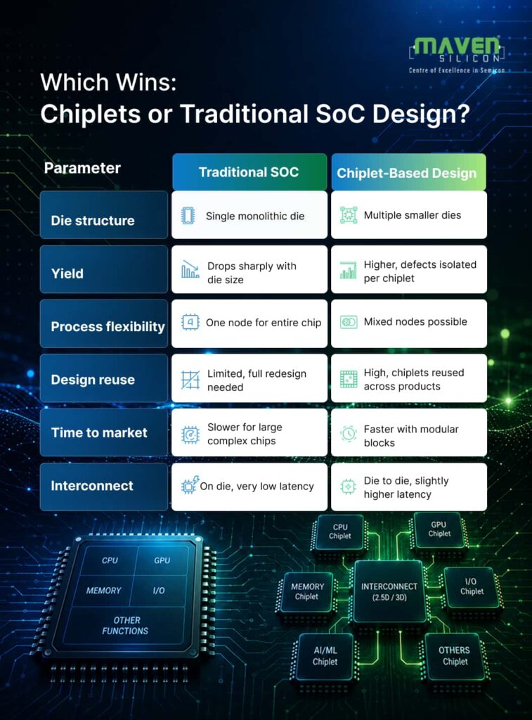
Which Wins: Chiplets or Traditional SoC Design?
Neither approach is universally better; the right choice depends entirely on what you are building. A traditional SoC integrates every function on one die, which keeps latency low and design simpler, but it locks you into a single process node and a single point of failure. Chiplet-based chip design trades some of that simplicity for flexibility, better yield, and mix-and-match economics.
Challenges with the Chiplet-Based Design Approach
Chiplets solve the cost and yield problem, but they introduce a new set of engineering challenges that a purely monolithic flow never had to deal with:
- Interconnect standardisation: Without a common die-to-die protocol, chiplets from different vendors simply cannot talk to each other. Efforts like UCIe exist precisely to solve this, but adoption is still maturing.
- Thermal management: Stacking dies in 2.5D or 3D packages concentrates heat in a small footprint, making thermal design and power delivery far harder than on a single flat die.
- Known-good-die testing: Every chiplet must be tested before assembly, since a single faulty die can ruin an otherwise expensive multi-die package.
- Assembly and packaging cost: Advanced packaging techniques such as CoWoS or Foveros add process steps and cost that partially offset the yield savings chiplets provide.
- Signal integrity across dies: Die-to-die links must preserve bandwidth and low latency despite crossing package boundaries, which demands careful physical design.
- EDA and tool maturity: Multi-die design, verification, and thermal co-simulation tools are still catching up to the complexity that chiplet systems introduce.
Industry Standards Shaping Chiplet Design
Interoperability between chiplets depends on shared standards and vendor packaging technologies. Currently, UCIe is the most widely discussed open die-to-die interconnect standard, but it is far from the only relevant technology:
| Standard / Technology | Owner | What It’s For |
|---|---|---|
| UCIe | Open industry consortium | Open die-to-die interconnect standard for chiplet interoperability across vendors |
| Bunch of Wires (BoW) | Open Compute Project | Open-source, low-cost die-to-die PHY aimed at organic substrates |
| OpenHBI | Open Compute Project | Open high-bandwidth interconnect spec for chiplet-to-chiplet links |
| Intel EMIB | Intel | Embedded silicon bridge for 2.5D packaging without a full interposer |
| TSMC CoWoS | TSMC | Chip-on-wafer-on-substrate 2.5D packaging widely used for AI accelerators |
| TSMC SoIC | TSMC | 3D stacking technology for die-on-die integration |
| Intel Foveros | Intel | 3D die-stacking packaging technology used in client and data-centre products |
| Samsung X-Cube | Samsung | 3D IC stacking technology combining logic and SRAM dies |
Real-World Examples of Chiplet-Based Design
The theory behind chiplets is easier to grasp with concrete products that already ship at scale. The article would be much stronger with examples such as:
- AMD Zen processors (Core Complex Dies + I/O Die): AMD’s Ryzen and EPYC families separate compute cores from I/O onto different dies fabricated on different nodes.
- AMD Instinct MI300 (3D chiplet architecture): combines CPU, GPU, and HBM memory chiplets in a single 3D-stacked package for AI and HPC workloads.
- Intel Ponte Vecchio: a GPU built from over 40 chiplets using Foveros and EMIB packaging, aimed at supercomputing.
- Intel Meteor Lake: Intel’s client processor line that splits compute, graphics, SoC, and I/O into separate tiles connected with Foveros.
- NVIDIA Grace Hopper Superchip: couples an Arm-based CPU chiplet with a Hopper GPU chiplet over a high-bandwidth, low-latency link.
- AMD EPYC processors: a widely cited example of chiplet-based server CPUs that scale core counts economically across generations.
These examples illustrate why different chiplet-based approaches are used, the right packaging and interconnect choice depends on the performance, cost, and power targets of the product.
What is India’s Role in the Chiplet Ecosystem?
India is no longer just a services hub for the semiconductor world, it is building genuine design capability. The government’s semiconductor mission has pushed indigenous chip design, EDA tool access, and workforce training as national priorities. India’s semiconductor market has grown from roughly USD 45 to 50 billion in 2024-25 and is projected to reach USD 100 to 110 billion by 2030, according to India’s Ministry of Electronics and IT.
- Design Linked Incentive schemes are funding domestic chiplet and IP design startups.
- Global firms are expanding their India based VLSI design and chip design centres in Bengaluru, Hyderabad, and Noida.
- A growing pipeline of skilled engineers is what makes this expansion possible, starting with strong foundational training.
Where Are the Opportunities for Engineers in Chiplet Design?
Chiplets have created an entirely new set of engineering roles, several of which barely existed a decade ago.
| Role | What You Would Do | Typical Background Needed |
|---|---|---|
| Die-to-die interconnect engineer | Design and verify UCIe or custom interconnect protocols | Digital design, protocol verification |
| Advanced packaging engineer | Work on 2.5D/3D packaging, interposers, and thermal design | Physical design, packaging fundamentals |
| Chiplet verification engineer | Verify individual chiplets and system level integration | UVM, SystemVerilog, functional verification |
| System integration architect | Define how multiple chiplets communicate as one system | SoC architecture, high speed interfaces |
| DFT engineer for chiplets | Ensure each die and package can be tested | Design for testability, ATPG |
Which Skills Do You Need to Work with Chiplet Technology?
- Digital design and RTL fundamentals: you cannot design a chiplet without understanding the block it represents.
- Advanced packaging knowledge: 2.5D, 3D, interposers, and thermal management are now core skills, not niche specialities.
- Protocol and interconnect expertise: familiarity with UCIe and die-to-die interfaces matters.
- Functional verification: SystemVerilog and UVM skills matter even more in a multi-die system.
- Design for testability: testing a multi-die package is trickier than testing one, so DFT knowledge carries weight.
A recognised semiconductor certification alongside hands-on lab experience gives you a genuine edge with recruiters. Maven Silicon’s advanced VLSI physical design and verification programme covers several of these areas.
What Does the Future Hold: 2026 and Beyond?
Expect chiplets to move from a high-end HPC and AI niche into mainstream consumer and automotive silicon over the next few years. Standardisation around interconnect protocols will make it easier for smaller design houses, alongside giants like AMD and Intel, to build chiplet-based products.
- Open standards will lower the barrier to entry for chiplet-based chip design.
- India’s expanding design ecosystem will likely produce homegrown chiplet IP within this decade.
- Automotive and edge AI will become major chiplet adopters, demanding scalable, cost-efficient compute.
- Engineers who combine design skills with packaging and system-level thinking will be the most employable talent here.
Conclusion and Next Steps
Chiplets are reshaping how the world designs and builds silicon, and this shift is not slowing down. Whether you are a student trying to understand where the industry is headed, or a professional planning your next move, understanding this modular approach is no longer optional. The semiconductor industry is rewarding engineers who understand both classic chip design and this newer, modular way of building systems.
If you are ready to build these skills properly, explore Maven Silicon’s VLSI and Embedded Systems courses and take your first real step toward a career in chip design.
Reference links :-
https://www.marketsandmarkets.com/Market-Reports/chiplet-market-131809383.html
https://www.pib.gov.in/PressReleasePage.aspx?PRID=2224839®=3&lang=1

Share This Post:


75,221
SUBSCRIBERS
Subscribe to our Blog
Get the latest VLSI news, updates, technical and interview resources
