VLSI Industry
Semiconductor Industry 2.0 | Maven Silicon
 August 10, 2021
 5 minutes read
 4501 Views


Everything is changing in the Semiconductor Industry to keep pace with 50 years old Moore’s law, the number of transistors in a chip doubles about every two years. In this article, I am delighted to address this question ‘Where are we heading?’ and explain how the semiconductor industry is evolving to support new technologies like AI, especially for the aspiring electrical and electronics engineers who want to be the next generation of chip designers.
We are heading towards the smart world that offers smart homes, smart cities, and industrial and business automation through IoT and Artificial Intelligence. It’s possible primarily because of new and powerful chips that we make with the use of advanced fabrication processes, along with new and powerful software applications that we create with the help of advanced software programming languages and methodologies.
Let us recollect how our journey has been with the evolution of chip design. The invention of Integrated Circuits made our life integrated with Music systems, Telephones, and Television two or three decades back. If you recollect your memories, later on, personal computers became popular and replaced many devices like music systems and typing machines and introduced automation in every business and industry. Then we transformed the PCs into laptops mainly through the advancement of chip design technology like SoC [System-On-Chip] design. With this experience, we were able to create smartphones and tablets. It has empowered every common person to create and share data with the world, mainly with the help of the internet through social media platforms like Facebook, YouTube, WhatsApp, Twitter, etc. So, I would say that the advancement of software programming technologies on par with chip design advancement has helped us reach this current state.
Naturally, this empowerment [Powerful Hardware + Powerful Software] leads us to realize the smart world by evolving technologies like the Internet of Things and Artificial Intelligence. So, let me explain how this new era of automation is going to transform the semiconductor industry.
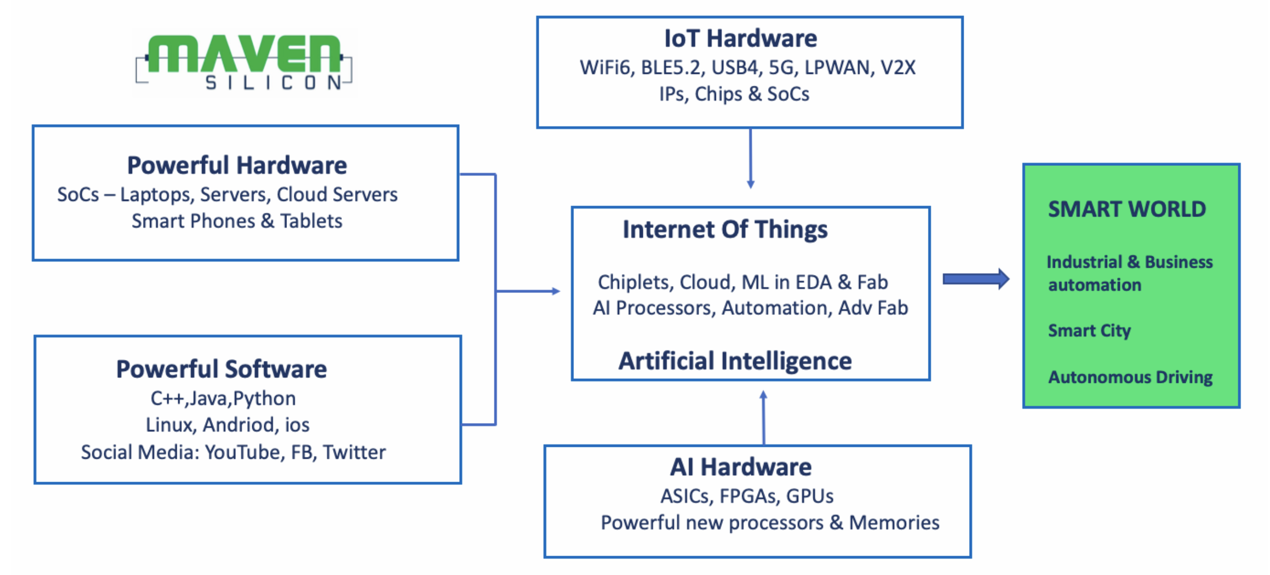
Internet of Things [IoT/IoE] demands new standards of connectivity protocols WiFi6, BLE5.2, USB4, 5G, LPWAN, V2X, etc., to realize the Industrial Automation, Smart City, Autonomous Driving, etc. In order to support the new standards and protocols, we chip designers need to design and create unique IPs, Chips, and SoCs at higher technology nodes. Some automotive and industrial chips may demand a specialized fabrication process, as they may be used in extreme environments.
Artificial Intelligence demands powerful processors and memories to realize applications like Autonomous Driving, Natural Language Processing [NLP], Machine Learning [ML], etc. The growth and amount of real-time data collected from the IoT-enabled devices and the advancement of machine learning algorithms on devices and the cloud will lead to the development of AI-based applications. NLP, automation, and trust are the three main themes that will shape the advancement of AI.
At present, AI experts are open to trying everything, new & existing processors, FPGAs, GPUs, etc. For some mathematical intensive applications, they find that FPGAs are better than ASICs. As long as their software works fine at high throughput and optimal power and they are fine to try and use any piece of silicon, ASIC/FPGA, to create the AI application at the right cost. So, I would say the evolution of new and custom processors and memories can only help AI experts standardize the implementation process and create many new AI applications at an optimal price.
It’s obvious that the evolution of AI and IoT demands new and powerful Chips and SoCs that have sensors and analog IPs along with digital IPs and sub-systems. Integrating sensors, analog modules with digital logic becomes impossible due to process incompatibility and limitations. So, in the semiconductor industry, we are also exploring the options of creating such powerful SoCs through new design approaches like Chiplets in addition to the monolithic design process. As the monolithic SoC scale-up is expensive, we make the SoCs by directly connecting the chips which have already been fabricated at different technology nodes. There are several approaches to chiplets. The basic idea is that you have a menu of modular chips, or chiplets, in a library. Then, you assemble chiplets in a package and connect them using a die-to-die interconnect scheme. In theory, the chiplet approach is a fast and less expensive way to assemble various types of third-party chips, such as I/Os, memory, and processor cores, in a package.
Also, we opt for the cloud to design such complex SoCs that demand more computation during simulation or implementation. During peak load on the server firm, especially while doing multiple tape-outs, any regression simulation or physical verification like DRC, LVS, etc., may demand infinite additional hardware resources to sign-off the verification and meet TTM. So naturally, we move towards using the cloud for the chip design similar to software programming. The EDA industry also offers cloud-based EDA solutions, addressing the IP security challenges. It helps the chipmakers, especially start-ups, focus on innovation through experimenting with new architectures and interfaces for their new chips with limited resources rather than setting up expensive on-premise emulation and simulation farms.
We also use ML algorithms to improve the EDA process and do the chip design efficiently. ML algorithms enhance the EDA tool algorithms to automate and improve the performance in some areas like test generation, synthesis, physical design, etc. For example, the EDA uses machine learning to analyze the performance & power consumption of various CPU implementations using the same set of fundamental building blocks. So, the evolution of Artificial Intelligence would transform the EDA and chip design process towards realizing our dream ‘AI designs it’s AI chip’.
References: Wikipedia, Design&Reuse, Semiconductor Engineering

Share This Post:


75,221
SUBSCRIBERS
Subscribe to our Blog
Get the latest VLSI news, updates, technical and interview resources
