DFT
What is Memory Test & Repair in VLSI?
 July 6, 2023
 6 minutes read
 16223 Views


What is a Memory test?
Memory test in VLSI is the process of testing the functionality of the memory blocks in an IC during the manufacturing test. Memory testing is performed using dedicated DFT instruments that generate test patterns applied to the memory under test and then compare the stored data with the expected results.
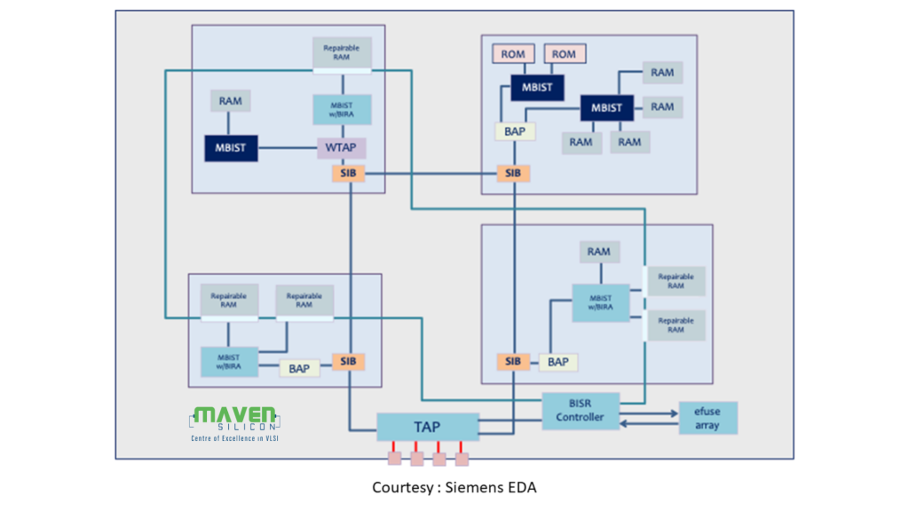
MBIST architecture at the chip level
Memory faults
A memory test algorithm is a finite sequence of test elements used to test the memory cell. The test elements consist of the following:
- Memory read or write operations
- Data patterns
- Address information’s
The test time (complexity) of an algorithm is expressed in terms of N (N = memory size)
Higher complexity means longer test time.
Algorithms like the March algorithm are used for detecting memory faults.
Faults detected by the March algorithm
- Stuck-At Faults
- Stuck-Open Faults
- Transition Faults
- Destructive read Faults
Stuck-At Faults
In this model, a memory cell is permanently forced to a logic 0 (stuck-at-0 fault) or logic 1 (stuck-at-1 fault) value irrespective of any value written to the cell.
How to detect Stuck-At Faults?
A logic 1 must be read from the cell under test to detect the stuck-at-0 fault while a logic 0 must be read to detect the stuck-at-1 fault.
Stuck-Open Faults
In this model, a memory cell can’t be accessed which could be due to an open word line.
How to detect stuck-Open Faults?
The faulty memory cell can have either x or 1.
Transition Faults
In this model, a memory cell fails to undergo a transition from a logic 0 to a logic 1 value (up transition fault) or from a logic 1 to a logic 0 value (down transition fault). These faults are special cases of stuck-at faults because once the non-faulty transition occurs, the faulty cell can no longer transition and hence behaves like a stuck-at fault.
How to detect Transition Faults?
To detect an up-transition fault, the following sequence of events must occur
- The cell under test must be storing a logic 0.
- Logic 1 must be written into the cell.
- The cell must be read before a logic 0 is written to it.
To detect a down transition fault, the following sequence of events must occur
- The cell under test must be storing a logic 1.
- A logic 0 must be written into the cell.
- The cell must be read before Logic 1 is written to it.
Destructive read faults
This fault can cause the contents of a memory cell to be changed during read access. However, the value read after the first read access could be the correct value.
How to detect Destructive read faults?
To detect a destructive read fault, the cell under test must be initialized and then read multiple times in consecutive clock cycles.
March algorithm
The March test algorithm has a sequence of March elements. Each element is specified by two important things as mentioned below:
Operations & data
- Writing 0 to a cell(w0)
- Writing 1 to a cell (w1)
- Reading an expected 0 (r0)
- Reading an expected 1 (r1)
Address sequence
- Address changes in ascending order
- Address changes in descending order
March algorithm notation
(w0); (r0, w1); (r1)}: This sequence has a complexity of 4N i.e. write 0, read 0, write1, read1
Notations used in the algorithm
R0 – Read the current location and compare the most significant output bit to 0
R1 – Read the current location and compare the most significant output bit to 1
W0 – Write to the current location, applying 0 to the least significant input bit
W1 – Write to the current location, applying 1 to the least significant input bit
A – Number of address locations
R – Number of row address locations
C – Number of column address locations
Memory Repair
Memory repair is a process of correcting defects in the memory blocks of an IC that are identified during memory testing. Such memories should be repairable memories.
A RAM with redundancies & reconfiguration circuit is called a repairable RAM. The built-in self-repair (BISR) technique has been widely used to repair such repairable RAM thus enhancing the yield of memories with the redundancy logic. Repairable memories have redundant memory locations i.e. spare rows & columns.
Self-Repair Architecture
- Repairable memory
- Built-in self-repair circuit (BISR)
- Built-in repair analysis (BIRA)
Major components
- Repairable RAM with a repair access port
- BIST circuit
- BISR circuit
- Fusebox
Self-Repair Architecture
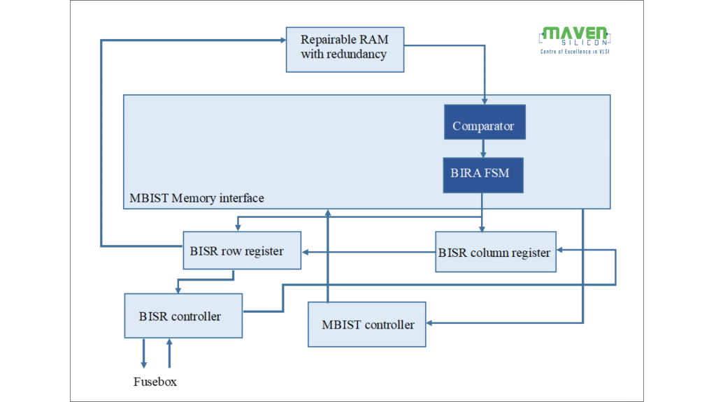
Procedure for Memory Repair
- During memory testing, a comparator is used to identify memory status by comparing the golden reference value with the actual data from the memory.
- Based on the comparator status and some interface signals, BIRA FSM will trigger and start collecting the failure information from the memory i.e.(Failed row & address).
- The BIRA FSM determines which failures can be repaired using the given redundant rows and columns and computes the solution.
- The BIRA FSM generates the following signals
- RRA: Repair row address is the row address of the defective row
- RAE: Row address enable is the enable signal of the row multiplexers to skip the defective row and select the spare row.
- CRA: The column repair address is the column address of the defective column
- CAE: Column address enable is the enable signal of the column multiplexers to skip the defective column and select the spare column.
- The repair signatures are loaded into the fuse registers from the BIRA FSM & then shifted to the chain of the repair registers.
- The failing addresses are stored in the BISR registers and an address mapping procedure is used to bypass the faulty memory location.
- The BISR circuit has a chain of BISR registers that shifts the information to the BISR controller.
- The BISR controller compresses the content of the scan chain and writes to the fuse box.
- The Fusebox is a non-volatile memory that stores the memory repair information which will blow the fuse after the production test to get repair the memory.
Also read: DFT: Scope, Techniques & Careers
Conclusion
Memory testing is a crucial stage in the DFT world for embedded memories. Research on high-speed and high-density memories continues to progress. In the coming years, Moore’s law will be driven by memory technologies that focus on aggressive pitch scaling and higher transistor count. Needless to say, this will drive up the complexity of testing and make it more challenging to test memories without pushing up the cost. As discussed in the article, using the MBIST model along with the algorithms and memory repair mechanisms, including BIRA and BISR, provides a low-cost but effective solution.
Aspiring to become a DFT engineer? Explore our Job-Oriented Advanced VLSI Design and DFT Course with hands-on project experience and 100% placement assistance – Advanced VLSI Design and DFT Course

Share This Post:


75,221
SUBSCRIBERS
Subscribe to our Blog
Get the latest VLSI news, updates, technical and interview resources
